Applications of D 263®

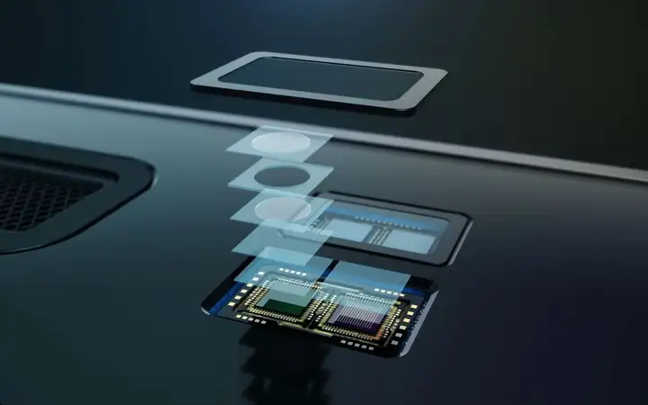
Camera imaging
The D 263® family of glasses are ideal for miniaturization, which is highly beneficial in areas such as camera imaging where components are becoming increasingly small and lightweight. The multi-functional D 263® T eco can act as an IR-cut filter substrate and Optical Low Pass Filter (OLPF) substrate in a variety of smartphone, computer and CCTV camera systems, as well as fingerprint sensors and touch panels.
Learn more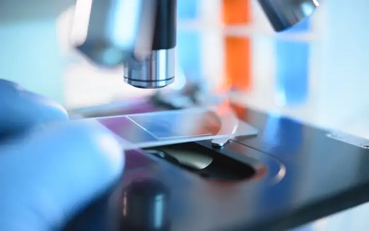
Microscopy cover glass
SCHOTT D 263® M is engineered for excellence in microscopy applications. It sets the benchmark for microscopy coverslips, currently being the only product on the market that meets the stringent ISO 8255-1 standards. Engineered for precision and superior optical performance, it ensures specimens are accurately positioned for stable, high-resolution imaging. Its advanced composition provides exceptional protection against contaminants and environmental factors, preserving slide integrity for both immediate examination and long-term storage
Learn more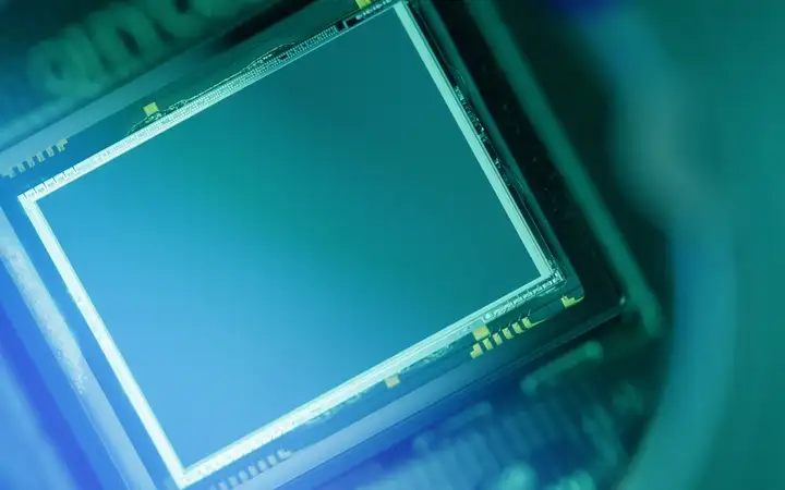
CCD and CMOS sensors
Image sensors that capture light and convert it into electrical signals are crucial components of cameras in smartphones, tablets and consumer cameras, as well as automotive cameras and machine vision systems. D 263® T eco is the preferred cover lid material for CMOS imaging sensors – now standard in the majority of optical devices – while D 263® LA eco is ideal for CCD technology and high-end CMOS equipment such as professional cameras.
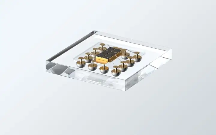
Semiconductors and MEMS
Versatile, multi-functional SCHOTT glasses such as D 263® T eco act as high quality covers or substrates for miniature MEMS devices within consumer electronics, biotech equipment and automotive systems. As an ultra-thin, lightweight glass, it also can be used as interposer substrates in semiconductor packaging, protecting tiny components and ensuring reliable long-term performance for a variety of modern technology.
3D Imaging and Sensing
D 263® glass is an essential material for wafer level optics and plays an important role in nanoimprint lithography technology. The stable technical properties of D 263® also helps structured light, time-of-flight (ToF) sensors, and stereo vision solutions to function at a high level. This enables technologies such as face recognition, distance detection, mobile payment, animation, 3D scanning, augmented reality (AR), and virtual reality (VR).
Learn more
RF and HF
D 263® serves as substrate or part of functional devices that enable or increase the performance of a large variety of RF and HF applications such as antennas and filters. D 263® is also increasingly used as a glass substrate in surface acoustic wave (SAW) filter systems in the growing 5G mobile communications sector.