Applications of FOTURAN® II
Thanks to its excellent versatility, structured FOTURAN® II is a key material in a large number of applications. Those applications include titer plates in microfluidics, power inductors in MEMS systems, and probe cards in semiconductors, as well as biotech and micro-optics components.
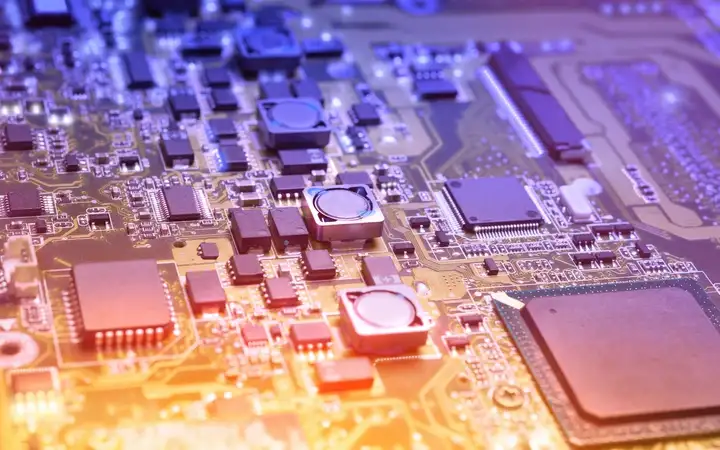
Semiconductors
Due to its excellent properties, FOTURAN® II plays an important role in semiconductor applications. Its easy structuring makes it highly compatible, while vias can efficiently be made on the FOTURAN® II substrate to a very high standard. These properties are used in components such as probe cards as an interface for the testing of functional semiconductor wafers.

Telecommunication
Components made of FOTURAN® II photo-structurable glass-ceramic can be more suitable for 5G applications than alternatives such as silicon. MEMS-based radio frequency (RF) passive components are often favored in 5G communications thanks to improved isolation, lower power dissipation, high integration and lighter weight. In such cases, structured glass-ceramic components offer benefits such as high insulation and low signal attenuation.

Micro-optics
SCHOTT FOTURAN® II has a vital role in micro-optics. After the post-processing stage, the suitability of FOTURAN® II for structuring makes it ideal for creating micro optical systems. 3D micro-optical components can be embedded in FOTURAN® II glass using a tightly focused FS laser beam or etching into the material structure – a process that’s useful in the production of optical waveguides.
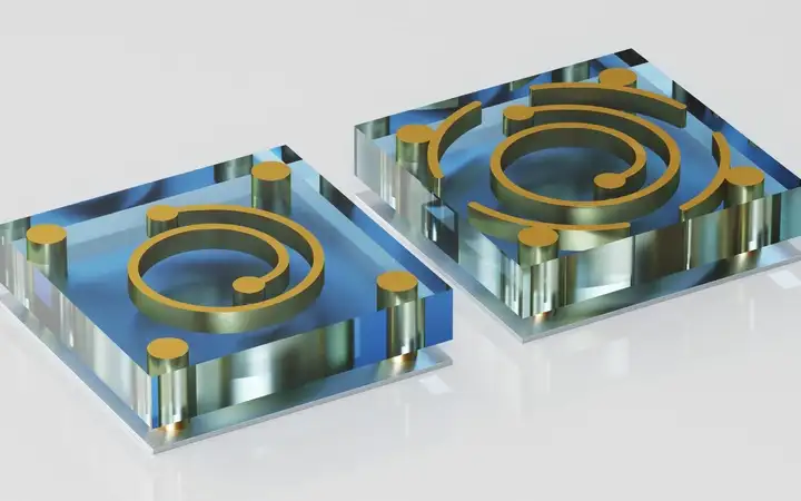
MEMS
MEMS inductors are relied upon in many areas of the electronics industry, and the emergence of power inductors promises to advance the field further. FOTURAN® II provides these devices with a small footprint (<0.75 mm per side), high Q factor and high self-resonance frequency. It also offers low-cost manufacturing, a wide range of inductances and high SRF (above 10GHz), along with current handling up to 5A.
Flow sensors and IC packaging
Many industries trust FOTURAN® II to power existing products. It is chemically stable compared to materials such as silicon, while its structurability provides flow sensors with small thermal masses, leading to ultra-fast response times. The ability of FOTURAN® II to create high-aspect-ratio TGVs also enables highly efficient production of IC packaging elements.

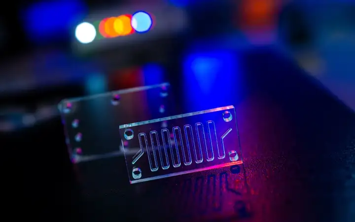
Biotech and micro-fluidics
FOTURAN® II is widely used in the biotech and micro-fluidics fields. Excellent optical transparency combined with low self-fluorescence plus high chemical stability and thermal resistance make it ideal for reusable, easy-to-clean titer plates, while it also facilitates complex structures with biocompatible design for biochip substrates. Elsewhere, it can also be used in the production of 3D micro-channels within materials.