Pressure sensors
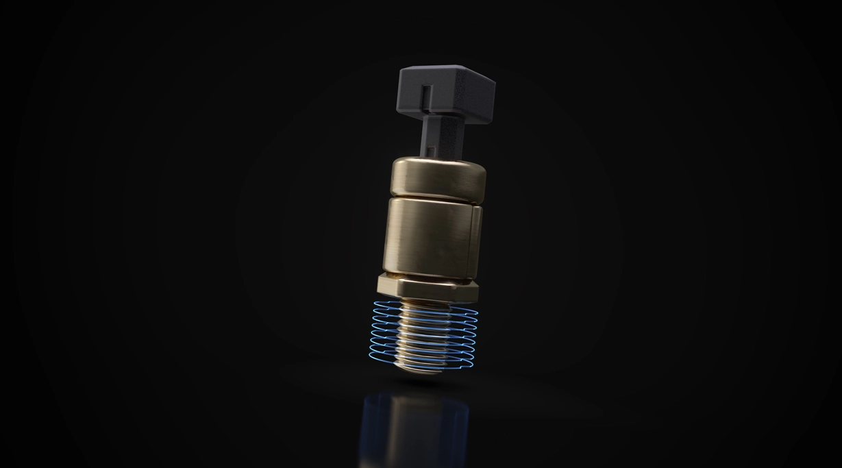
Pressure sensors operate under continuous mechanical load, where even small material changes accumulate over time. What starts as microscopic deformation or drift can eventually compromise measurement accuracy and system reliability. SCHOTT glass materials are engineered to maintain dimensional stability, mechanical integrity and long-term performance under these conditions.
This page focuses on how glass performance at critical system interfaces influences mechanical stability, dimensional control, and long‑term barrier integrity — key factors that directly define sensor reliability over time.
When pressure decides, materials make the difference
Pressure sensors face relentless mechanical stress. They must deliver precise, reliable data continuously – often for years – in environments that are chemically aggressive, thermally unstable or mechanically demanding.
In reality, pressure sensors rarely fail due to electronics or signal processing. They fail when materials drift, deform, age or lose integrity. This makes material selection a critical design decision.
No room for error in real-time pressure sensing
Pressure is not a momentary event. It is a constant condition.
Even mmaterial changes accumulate over time. Small deformations, microscopic leakage, or gradual drift may initially go unnoticed– until they compromise measurement accuracy, system safety, or operational trust.
Reliable pressure sensing requires materials that perform consistently over time, not just within initial specifications.
The core requirements of pressure sensing
Across industries, pressure sensing systems share fundamental requirements:
Unlike optical systems that can fail suddenly, pressure sensors degrade gradually. The material’s behavior ultimately determines how long measurement stability can be maintained.
Why pressure sensors fail over time
Pressure sensors do not typically fail suddenly. They fail gradually.
Common failure mechanisms include:
- Mechanical creep under sustained load
- Thermal expansion mismatches between materials
- Sealing interface degradation
- Stress-induced drift over extended use
Once deployed, these effects cannot be corrected through downstream signal processing. The material’s behavior defines the system’s operational limits.
Pressure sensing: No second chances
Unlike many electronic systems, pressure sensors cannot be continuously recalibrated without interruption. Once in service, material deformation, drift, or leakage cannot be corrected in real time.Pressure sensing puts material behavior on full display at the system level.
Measurement stability depends entirely on how materials perform under load – not on any downstream corrections.

Leak-tightness: A material challenge, not a marketing claim
Long-term leak-tight performance is often promised but rarely properly defined. Real-world performance is not determined by short-term test results, but by how consistently materials maintain barrier integrity under continuous mechanical stress, temperature cycles, and environmental exposure.
In pressure sensing systems, even microscopic leakage or gradual interface degradation accumulates over time. What seemed insignificant initially can eventually compromise measurement accuracy, system safety, or long-term reliability.
True leak-tightness depends on material stability at the interface level. It is not an optional feature – it is fundamental to sensor reliability.
Material stability: The foundation of pressure sensing performance
In pressure sensing applications, material properties are not just optimization factors. They determine how long a sensor remains reliable under constant load. Glass offers unique properties that maintain stability where other materials gradually deteriorate.
Key material properties that matter in pressure sensing
Why material behavior matters for real-time sensing
Real-time performance depends on predictability, not peak specifications. When material behavior remains stable, pressure signals stay reliable – without needing recalibration, compensation, or delay.
In pressure sensing, real-time performance starts with how materials behave under load, not with the electronics.
Glass: An active component in pressure sensing
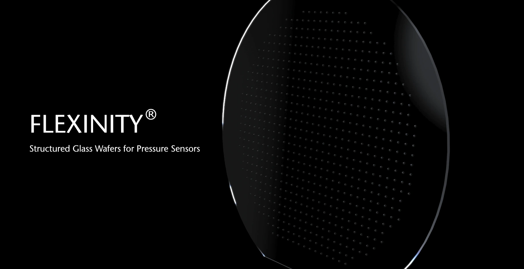
In high-performance pressure sensors, glass is far more than just protection. Its precisely controlled thickness, homogeneity, and surface quality enable defined mechanical deformation under pressure.
This reproducibility directly impacts:
- Consistent force transmission
- Stable measurement characteristics
- Uniform performance across production batches
Glass solutions for pressure sensing challenges
SCHOTT provides pressure sensor developers with material expertise and application-specific glass platforms that address the fundamental limitations of pressure sensing systems. Glass materials are used at critical system interfaces where mechanical stability, dimensional control, and long-term barrier integrity directly affect sensor reliability.Specialized glass platforms
Different pressure sensing applications require different glass solutions. Material selection should be based on system requirements, not default choices.MEMpax®
For high-stress pressure sensing applications requiring exceptional stability.MEMpax® excels in applications where pressure sensors face continuous mechanical loading and require long-term dimensional stability. Its defined mechanical characteristics ensure predictable performance and minimal drift throughout the sensor’s operational life.

D 263® T eco
For compact, scalable pressure sensor designs.D 263® T eco enables thin, compact sensor architectures with tight tolerances. Its superior surface quality and process compatibility support miniaturized designs and consistent performance in high-volume production.

BOROFLOAT® 33
BOROFLOAT® 33 combines thermal stability, mechanical strength, and excellent chemical resistance, making it ideal for demanding pressure sensor applications. Its low thermal expansion ensures dimensional stability and compatibility with silicon, enabling reliable bonding and long-term measurement accuracy even under varying temperatures and harsh conditions.
Small sensors, big material challenges
As pressure sensors become smaller, tolerances tighten, and material behavior becomes increasingly critical. Solutions that work at larger scales often fail when dimensions shrink.
Thin glass enables compact sensor designs without compromising mechanical stability or long-term barrier integrity. Its compatibility with scalable manufacturing processes ensures consistent measurement stability in high-volume production.
Built for the toughest conditions
Pressure sensors operate where materials face extreme challenges:
- Aggressive chemicals and fluids
- Dynamic pressure cycling
- Safety-critical operating conditions
In automotive, industrial, and medical applications, material degradation simply is not an option. Glass maintains its performance where other materials would swell, age, or break down.
Pressure sensing in context
Pressure sensing is part of a larger real-time sensing ecosystem where material behavior determines system stability.Automotive applications
Imaging systems
Mobile devices
Medical equipment
When pressure decides, material behavior matters
Continuous load, temperature changes and media exposure define how pressure sensors perform over time. Tell us about your application, and we will help you match it with glass properties that ensure stable and predictable performance.


