Semiconductor & Datacom
Unlock the future with specialty materials
Trends and challenges


Transforming semiconductors with specialty materials
SCHOTT contribution to advanced semicon packaging and front-end semiconductor manufacturing processes
At SCHOTT, our passion for innovation pushes the boundaries of technology. With world-class R&D expertise and an unmatched portfolio of specialty materials drive, we drive groundbreaking developments that transform industries and improve lives.
As a trusted partner, we provide industry leaders with the highest-quality materials and deep technical expertise – turning challenges into solutions. Together, we are shaping the future of technology.
Specialty materials: the catalyst for boundless innovation
From large panels for multi-chip integration to thin interposers with ultra-high TGV density near the die, SCHOTT empowers the semiconductor and datacom industries with a comprehensive range of specialty glass and materials. As trusted glass experts, we enable rapid advancements in cutting-edge technologies to unleash the future of high-performance.
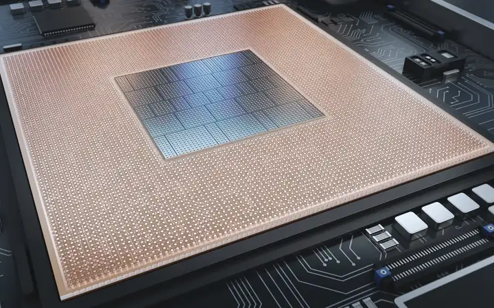
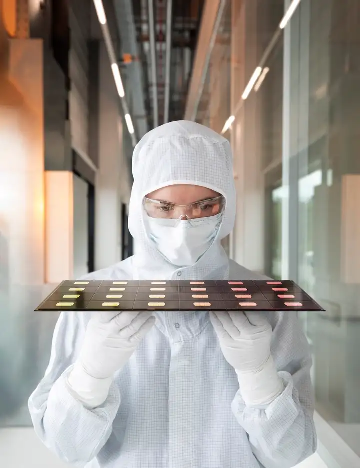
Advanced IC-packaging and integration
- Glass carrier: Wafers and panels for IC manufacturing and advanced packaging including fan-out wafer and panel level packaging (FO-WLP/FOPLP)
- Glass core substrate: Glass panels designed for structuring and lamination to create high-density advanced packaging substrates and interposers

Consumables for front-end processing
- Plasma etch equipment: Quartz materials serving as key materials for chamber components
- Epitaxy equipment: Quartz glass for components in epitaxy chambers
- Diffusion equipment: Fused quartz materials for diffusion processes

Lithography
- Display lithography: Glass in technologies for the production of displays
- IC lithography: Glass for applications in the manufacture of integrated circuits (ICs)

Sensors
- Pressure sensors: Glass in pressure monitoring of semiconductor processes
- Actuators: Glass in enabling long-term precision of piezoelectric actuators
- Gas sensors: Glass in environmental monitoring and safety applications
- Temperature sensors: Glass for fiber optic temperature sensing
- Positioning sensors: Fiber optic light guides for interferometric measurements

Optoelectronics
- Laser components: Glass for applications in data-communication and sensor technology
- Photodetectors: Glass for sensors for light detection
- LEDs: Glass in lighting and display technologies

MEMS
- MEMS packaging: Glass solutions for the encapsulation of MEMS components
- MEMS mirrors: Glass in optical systems and scanners
- Pressure sensors: Glass for pressure sensors in automotive and medical technology


High-frequency technology
- RF filters: Glass for high frequency filters in telecommunication applications
- Antennas: Glass in wireless communication systems
- Radar components: Glass in automotive and aerospace applications
Versatile specialty glass for advanced applications
Specialty glass is a remarkably versatile material that plays a vital role in high-tech industries. At SCHOTT, our materials range from ultra-thin and ultra-flexible to ultra-tough glass, designed to meet the demands of cutting-edge applications.
As a pioneer in specialty materials, we offer an extensive portfolio of materials and advanced processing capabilities – catering specifically to the semiconductor and datacom sectors.
High-purity quartz is a key material in semiconductor manufacturing, especially used throughout the front end process. Schott supplies quartz base materials ranging from standard purity to ultra-high purity and near net shape, customized to meet the requirements of advanced processes.
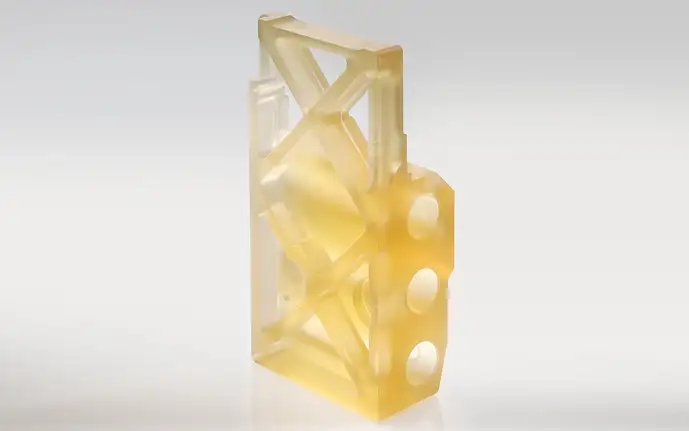
Substrates, wafers and panels
Substrates and wafers for semiconductor production.
- Carrier wafers
- Carrier panels
- Glass panels for glass core substrate
- Structured wafer (TGVs and cavities) prototyping
Glass optical fibers
Fiber optic solutions for optical sensing and metrology
- Flexible light guides
- Fiber optic sub-assemblies
- Flexible imaging bundles

Quartz glass base materials
High-purity quartz is essential for advanced semiconductor front-end processes. We offer a wide range of near-net-shape ring and component geometries – from high-volume production to single-piece lot sizes – supporting the consumable business of leading equipment manufacturers. Our processes and capacity are designed to absorb typical semiconductor demand swings, ensuring stable supply even in volatile market conditions.
-
Near-net-shape manufacturing
-
Etch rings (focus / edge / cover) for plasma etch equipment
-
Flanges and liners for epitaxy and diffusion equipment

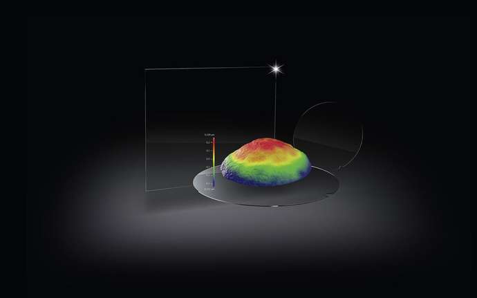
ZERODUR® glass-ceramic
ZERODUR® glass-ceramic delivers unmatched thermal stability for advanced lithography systems. Its near-zero thermal expansion ensures precise wafer positioning and consistent performance under extreme conditions. With exceptional homogeneity and mechanical strength, ZERODUR® is the foundation for critical components like reticle and wafer stages. Trusted in EUV lithography, it enables the accuracy required for next-generation semiconductor manufacturing.More about ZERODUR® glass-ceramic