Guiding photons for improved imaging and detection
Beyond fiber optics
What has been possible with SCHOTT fiber optic technology is now moving to the next level. Whether your starting point is a fiber optic plate (FOP), micro-channel plate (MCP), light pipe array (LPA), large diameter images guide, or a modular combination of the above, SCHOTT’s engineering experts are ready to collaborate with you on a customized solution.Multi-channel plate

What is a laser structured glass plate?
Laser structuring can create patterns or structures in materials such as glass with more precision than traditional technologies such as CNC processing. It also works on a smaller scale than traditional fiber optic technology. These intricate micro- or even nano-scale structures can be positioned with extreme precision, allowing photons to pass through to reach, for example, a sensor or detector.In the case of a fiber optic plate (FOP), light travels through a core-clad fiber. In contrast, in a micro-channel plate (MCP), light is transmitted through channels or holes (“filled” with air), often coated to further enhance the paths of the photons. For a light pipe array, light moves through glass, guided by structures filled with various materials other than air.
To determine which solution is the best for a specific application, photon management is optimized by taking into account all parameters that influence the light path.
How does a photon move through a light pipe array?

Benefits of laser structuring
SCHOTT has been working with laser structuring for several years and we are continuously developing our knowledge and competencies as the technology evolves. This offers our customers the following benefits:


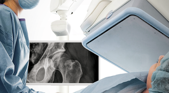
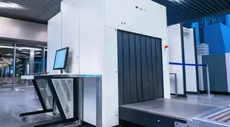
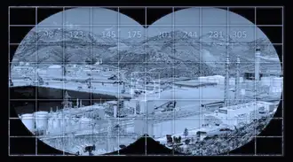
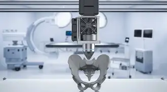
Application segments
Guiding photons with laser-structured functionalized plates offers options for a variety of industries.
Production process: Realizing laser-structured, functionalized plates
Three important phases in SCHOTT’s full end-to-end process lead to a large variety of designs and the creation of new solutions in optical path management for our customers‘ leading-edge applications.Glass development and manufacturing
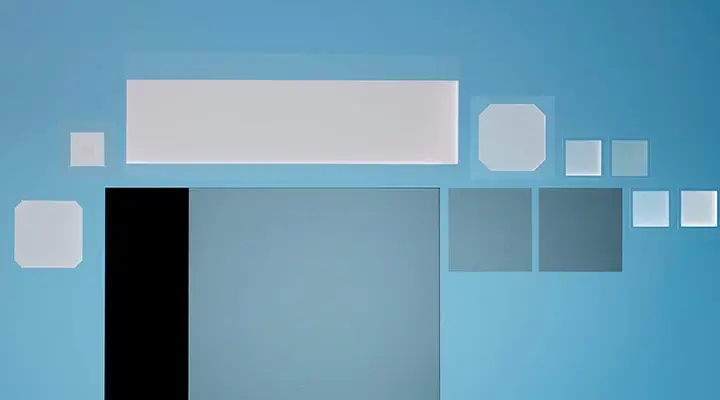
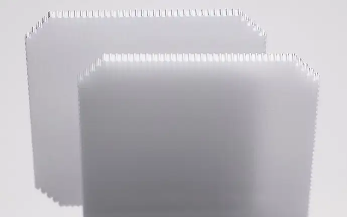
SCHOTT offers a broad portfolio of proprietary specialty glasses that we develop and manufacture in-house. Our glasses offer excellent performance, such as high optical transmission, and can be provided in a wide range of sizes, from very small to large formats up to 600 x 600 mm². Glass types include, for example, SCHOTT BOROFLOAT® 33, SCHOTT D263® T eco, and SCHOTT MEMpax®. Our various proprietary materials and depth of material knowledge allow us to design flexibly for the benefit of the customer.
In-house engineering and laser structuring
Thanks to our lasers and strong network of SCHOTT experts, we offer refined in-house engineering and design capabilities. Developing our laser competencies with the latest equipment technologies available on the market, we solve complex customer applications through multiple engineering disciplines. This allows us to become creative when laser structuring glass and developing application-specific solutions for our customers.
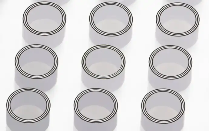
Pulsed lasers create structures in glass plates from simple to complex patterns, in nano- and micro-dimensions. There are numerous shapes that are now made possible with repeatable precision and accuracy. These range from tiny holes and extremely thin channels to optionally curved edges and angled channels. The design options are endless.
Further processing and functionalization
The functionality of the end-product depends on the secondary processing steps we provide. Based on SCHOTT’s in-house engineering expertise and our knowledge of glass and non-glass materials, we can offer a large variety of processing options. These include filamentation, ablation, functional coatings, interstitial deposition and atomic layer deposition (ALD), grinding and polishing, and many more.
Why choose SCHOTT?
SCHOTT‘s expertise in defining optical systems and guiding photons is based on 60 years of fiber optic knowledge.