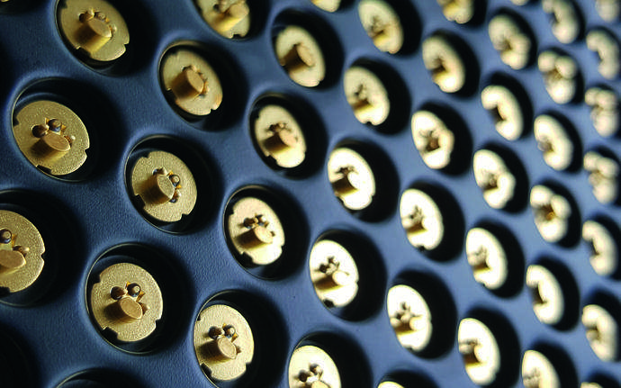
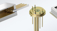
Illustration of a transistor outline (TO) package enabling data transmission

Transistor Outline (TO) Packages

SCHOTT’s hermetic transistor outline (TO) packages provide reliable encapsulation and protect sensitive semiconductor components from adverse effects. Perfectly matched TO headers and caps, as well as extensive customization possibilities, enable our customers to develop high-performance optical modules.
Illustration of a transistor outline (TO) package in an electronic circuit

Innovation leader in high-speed products

With more than 50 years of research and applied knowledge in the TO field, SCHOTT continues to be a leading force in designing and manufacturing innovative high-speed TO PLUS® designs that support next-generation data- and telecom infrastructure.

Tray full of transistor outline (TO) packages

Reliable quality for mass production

High quality and processability of TO components are essential to enable optimal throughput and superior performance. SCHOTT possesses vast knowledge that is essential for the production of these high-quality components.

Find your TO package

Find out which TO variant suits your needs and access detailed technical information by logging in to our interactive ‘TO Selector’.

HISENSE.png
News & Innovation stories

How Hisense is setting speed records with optical module technology

The era of 400G has arrived, and the optical communication industry is focusing on next-level speed. Dr. David Li, CTO of Hisense Broadband Multimedia Technologies, shares the challenges and opportunities in the datacom industry.

Read more

Want to know more? Let's talk

Whether you need more information, samples, a quote, or advice for a project, I would be delighted to talk to you.

Contact us
Robert Hettler, Head of R&D Opto-electronics at SCHOTT
Robert Hettler

Head of R&D Opto-electronics