Why next-generation chips need quartz glass built for extremes
Microchips are measured in nanometers, but making them depends on materials that can survive some of manufacturing’s harshest environments.

SCHOTT’s plasma-melted quartz glass can help chipmakers control purity and stability as semiconductor processes become more extreme.
- Making microchips means repeatedly exposing materials to heat, chemicals, and plasma.
- Quartz glass can help protect the controlled environments where chips are made.
- In plasma etching, impurities, micro-defects, or instability can affect process consistency and yield.
- Ilmasil™ fused quartz supports high purity, dimensional flexibility, and repeatable performance.
A finished microchip may look clean and almost impossibly small. But making one means exposing materials to heat, chemicals, and plasma again and again. It is one of the harshest environments in modern manufacturing. For Hartmut Zahel-Mahlberg, Managing Director of SCHOTT’s quartz glass business field, those extremes are just part of the job.
“Quartz glass is a material for extremes,” he says. “It’s very pure, heat resistant, and chemically reliable.”
In semiconductor manufacturing, those qualities have practical consequences. They can affect whether a process runs consistently or whether contamination, instability, or material failure leads to defects.
Walk the Talk – Hartmut Zahel-Mahlberg Pt 1
Modern microchips are built from structures measured in nanometers. The smaller those structures become, the less room there is for error. A particle too small to see, a trace impurity in the wrong place, or a component that behaves unpredictably under heat and chemical exposure can affect the precision of the process itself.
Hartmut explains the level of purity is through a familiar object. “To understand the purity, imagine 1,000 kilograms – one ton – of material,” he says. “Within that, the maximum amount of impurities would be about the size of a sugar cube.”
In many industries, that level of purity would be exceptional. In advanced semiconductor manufacturing, it is increasingly a baseline expectation.
Where quartz glass meets the microchip
Before a chip can do anything useful, it has to survive manufacturing. Wafers are patterned, layered, etched, cleaned, heated, inspected, and processed again and again. Each step depends on equipment materials that can hold up under demanding conditions without interfering with the wafer itself.
“Every chip produced – whether for mobile phones, PCs, or cars – sees quartz glass multiple times during production,” Hartmut says. “And that’s because of what the material can withstand.”
Take plasma etching, for instance. This step in semiconductor chip production uses energized gases to remove material from a wafer with extreme precision. In simple terms, it helps carve and define the tiny structures that allow integrated circuits to function.
“It’s a very aggressive chemical environment that allows no impurities,” Hartmut explains, “because that is where those tiny microstructures of integrated circuits are formed.”
If a quartz component contains impurities, those impurities can become a source of contamination. If a material contains micro-defects, those defects can affect how it responds to aggressive plasma exposure. If a part lacks mechanical stability, it can make an already sensitive process harder to repeat.
At nanometer scale, minor variation is no longer minor. Yield – the share of usable chips that make it through production – depends on keeping the process stable from one run to the next. Materials that survive harsh manufacturing environments without adding new risks are part of that stability.
Engineering quartz glass for harsher processes
SCHOTT’s Ilmasil™ fused quartz is produced through a plasma-based fusion process designed for demanding high-temperature and semiconductor applications. Purity matters, but so does how the material is made.
“What makes it unique is really the melting process,” Hartmut says. "It's a process that sets SCHOTT apart."
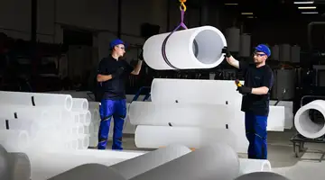
That melting process allows SCHOTT to produce heavy-walled hollow cylinders, also known as billets, in a single step. From there, the material can be processed into tubes, cylinders, or customized quartz components.


Equipment requirements vary widely in semiconductor manufacturing. A chamber component for one process may need a different size, geometry, or material behavior than a component for another. The material has to perform under stress, but it also has to fit the process.
“For our customers, the advantage is flexibility, especially in dimensions,” Hartmut says. “We can tailor the outer diameter, inner diameter, and wall thickness to their needs.”
That flexibility has a practical effect. “We don’t need to produce oversized material for the customer,” he continues. “Oversize means waste. And waste means extra cost.”
In semiconductor manufacturing, small differences can matter at large scale. Producing closer to the needed shape can reduce unnecessary processing, while a more consistent material can help protect yield and reliability.
The material behind the process
In the world of advanced computing and AI-powered chips, transistor counts and processing speed tend to get the attention. Materials usually do not.
Quartz glass does not become part of the finished chip, but it helps keep the manufacturing environment stable while the chip is being made. As plasma processes become more demanding, survival is not enough. Materials inside the equipment have to remain stable and resist contamination, even after repeated exposure to heat, chemistry, and plasma.
Walk the Talk – Hartmut Zahel-Mahlberg Pt 2
SCHOTT’s plasma-melted quartz glass is built around those requirements from the start. It is made for purity and stability, but also for the dimensions and repeatability semiconductor equipment requires.
Most people will never see the quartz glass involved in making their chips. But as semiconductor processes become harsher and more precise, existing materials cannot simply be stretched further. They have to be rethought for the conditions ahead.
“Material innovation – that is the work ahead,” Hartmut says. “Developing new materials with the purity, stability, and reliability required as semiconductor manufacturing pushes further into extreme process conditions.”