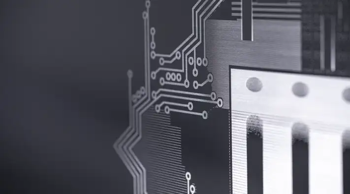
How glass enables next-generation semiconductor manufacturing
Inside the precision, materials science, and human expertise behind the glass carrier wafers that support today’s most advanced semiconductor processes.

Glass carrier wafers provide the mechanical, thermal, and optical stability needed to support today’s most advanced semiconductor processes.
- As chips become thinner and more complex, carriers stabilize wafers through critical steps like thinning, bonding, and debonding.
- Their engineered glass compositions are tuned to match each customer’s process flow.
- Manufacturing them requires a tightly controlled sequence of cutting, grinding, polishing, and inspection.
- These refinements ultimately help fabs improve precision, consistency, and overall yield.
Before the machines warm up – before a single wafer is processed – Da Ning begins his day with calibration. “A typical day’s work includes processing, measurement, analyses, adjustment, and validation,” he says. “The entire process requires dozens of steps, hundreds of inspections, and the dedication of a team that refuses to compromise.”
Modern semiconductors demand extraordinary consistency. As Senior Manager of Global Product Management, Da Ning and his team are responsible for producing the glass carrier wafers that make that level of precision possible. The challenge isn’t just creating a perfect piece of glass – it’s reproducing that perfection across every wafer, day after day, in a market where microscopic variation can compromise an entire lot.
For Da Ning, this level of care is both routine and deeply personal. “Working with glass and precision manufacturing is what first attracted me to this field,” he says. “Glass is an incredibly versatile material, and we’re pushing the limits of what it can do. It’s exciting to build a high-end product that helps customers realize their next-generation designs.”
Glass carriers don’t appear in the final chip. They aren’t mentioned at keynote events. Yet in an era defined by thinner devices, denser packaging, and increasingly complex architectures, they provide the stability that enables high-yield semiconductor manufacturing.
What is a glass carrier wafer?
At their core, glass carrier wafers are rigid, highly uniform support structures that hold extremely thin semiconductor wafers during processes such as thinning, patterning, bonding, and debonding. Their job is simple to describe but difficult to achieve: “These are very precisely manufactured pieces of glass that provide mechanical and handling support to semiconductor wafers and packages through steps that would otherwise damage them,” explains Colin Schmucker, Sales and Product Manager for Semicon Glass Solutions at SCHOTT.
Glass carrier wafers must remain stable through exposure to heat, vacuum, chemicals – and in many cases, UV-based debonding. From there, customer needs vary widely. “We work with manufacturers to evaluate trade-offs across parameters such as coefficient of thermal expansion (CTE), UV transparency, thickness options, and cost,” Colin continues. Each property determines how well the carrier pairs with the customer’s semiconductor materials and temperature profile.
In an industry operating at a scale where even the smallest dimensional drift can cascade into yield loss, these parameters are critical. When wafers are thinned to tens of microns – or bonded into complex 3D stacks – the carrier must behave exactly as expected.


Precision that builds on itself
Creating a glass carrier wafer is an exercise in cumulative precision. It begins with identifying the right glass composition. “In general, addressing specific CTE, physical, and optical properties comes down to identifying the correct glass composition,” Colin says. “We have a wide range of compositional space that can address combinations of required properties.”
This enables SCHOTT to “tailor solutions to temperature profiles, laser wavelengths, and bonding chemistries, Colin says, “all depending on the needs of a customer’s process flow.”
With the composition selected, the transformation unfolds in controlled increments. Every tool – cutting, grinding, polishing, cleaning – must be calibrated with micron-level accuracy. Every machine must be verified. Temperature and humidity must be tightly controlled.
“We carefully process wafers step by step, inspecting them with high-resolution metrology tools throughout,” Da Ning explains. “The glass is cut, ground, and polished through multiple stages, each one improving thickness tolerance, TTV, and flatness.
“Every wafer is tracked, inspected, and logged,” he continues. “And each step is a safeguard against deviation.”
As semiconductor manufacturing becomes more advanced, the expectations placed on carrier materials grow in parallel. Requirements now reach deeper into the details: tighter flatness windows, more stringent surface quality, transparency tuned to specific laser wavelengths, and mechanical properties optimized for ultra-thin handling.
“Device fabrication is very expensive,” Colin notes. “If improving the flatness, or transparency at a specific wavelength, or the Young’s modulus of a material results in even a marginal yield improvement in a fab, it’s well worth it for customers.”
A stable foundation for what comes next
The materials that support the semiconductor industry rarely make headlines. Yet without them, many of today’s most advanced processes would not be feasible.
Glass carrier wafers provide the stability needed to thin, align, bond, debond, package, and inspect the devices that power modern electronics.
For Da Ning, the work is more than technical – it is a craft refined through nearly two decades immersed in glass science and precision manufacturing at SCHOTT.
“The work we do isn’t just about making something,” he says. “It’s about mastering a process that demands respect, patience, and relentless attention to detail.”
And when he holds a finished carrier wafer – absent from the final chip but essential to its creation – it reflects the years of disciplined work and technical mastery that make today’s most complex technologies possible.