SCHOTT launches “Semicon next” knowledge hub to support the next generation of semiconductors enabled by glass
Thursday, 21 May 2026, Germany, Mainz
- As the semiconductor industry accelerates the adoption of glass-based solutions, SCHOTT launches “Semicon next”, an expert‑led knowledge hub to provide specialty material insights from lab development to mass production.
- Following the release of the first episode, the series will continue to address key topics that emerge as a real-world project evolves, from the limits of transistor scaling to material performance and pathways to industrial adoption.
- Backed by 140+ years of specialty glass expertise and real collaboration across the semiconductor value chain, the content covers deep-dive videos, whitepapers, and exclusive additional content.
As the semiconductor industry accelerates the adoption of glass-based technologies driven by demanding AI and high-performance computing (HPC) applications, SCHOTT is launching Semicon next, a freely accessible knowledge hub dedicated to specialty materials for next‑generation semiconductor architectures. The platform provides engineers and technology leaders with expert-led insights into how glass can unlock new design options beyond Moore’s Law and support scalable, high‑performance semiconductor systems – completely free of charge.
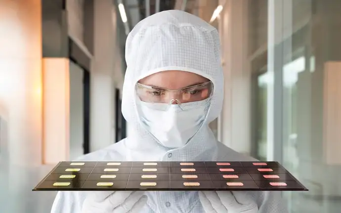
Today, leading semiconductor innovators have begun developing glass-based solutions and investing in production. This growing momentum reflects a fundamental shift: as traditional scaling approaches reach their limits, advanced packaging and system integration have become key differentiators for performance, power efficiency, and cost. Specialty glass is increasingly seen as a critical enabler for this next phase, but many questions remain around the materials, development, and manufacturability.
SCHOTT Semicon next addresses these questions head‑on. Following the release of the first episode, the series will continue over the coming months with deep-dive content covering topics from the limits of transistor scaling, material performance and pathways to industrial adoption. Designed as an evolving resource, the platform can be revisited as real-world projects progress. It provides in-depth insights into how glass-based solutions move from early development and prototyping to validated, production-ready processes—serving as a long-term technical reference hub for material science.
“Our new knowledge hub, Semicon next, is designed to help our customers move faster from idea to implementation, by turning material expertise into practical guidance for engineers facing the realities of advanced packaging,” said Dr. Christian Leirer, Head of Semicon Glass Solutions at SCHOTT. “By bringing the latest insights on glass-based solutions into one freely accessible hub, we want to start fruitful exchanges across the value chain and help teams push beyond today’s boundaries in performance, power efficiency, and cost.”
Trusted material expertise shaped by real manufacturing
With more than 140 years of specialty glass expertise and close contacts with leading players in the semiconductor industry, international technology group SCHOTT brings a real‑world perspective to the series. The company, which was founded by the inventor of specialty glass, Otto Schott, works across nearly every segment of the semiconductor industry, with decades of experience in microlithography and optical materials, dedicated technology platforms for glass core substrates and advanced carrier applications, and structured support for through‑glass via (TGV) development, prototyping, and validation. Backed by global application engineering teams in Europe, the United States, and Asia, SCHOTT translates material innovation into scalable solutions developed in close collaboration with customers.
SCHOTT Semicon next brings this expertise together in one place, delivering insights shaped by real manufacturing challenges and collaboration across the value chain, helping semiconductor teams make informed decisions as glass technologies move from emerging innovation to industrial adoption. Access to the new knowledge hub is free, while in-depth videos and whitepapers require a free registration. You can access SCHOTT Semicon next here.
About SCHOTT
International technology group SCHOTT produces high-quality components and advanced materials, including specialty glass, glass-ceramics, and polymers. Many SCHOTT products have high-tech applications that push technological boundaries, such as waveguides for augmented reality smart glasses, glass-ceramic mirror substrates in the world's largest telescopes, and laser glass in nuclear fusion research. With a pioneering spirit, SCHOTT’s 17,400 employees in over 30 countries work as partners across industries such as healthcare, home appliances, consumer electronics, semiconductors, optics, astronomy, energy, and aerospace. In fiscal year 2025, SCHOTT generated sales of EUR 2.83bn and an EBIT of EUR 230m. Founded in 1884 and headquartered in Mainz, Germany, SCHOTT is owned by the Carl Zeiss Foundation. As a foundation-owned company, SCHOTT pursues long-term innovation and conducts its business with a strong sense of social responsibility, reinvesting its success into the advancement of science and society. Learn more at SCHOTT.com

Yixuan Jin
PR-Manager