Applications of AF 32® eco
AF 32® eco provides solutions across the fields of consumer electronics, optics, semiconductors, MEMS, RF, and microdisplay. With a coefficient of thermal expansion matching that of a silicon wafer, AF 32® eco is an adaptable and reliable choice for a broad range of packaging applications.

 sensors")
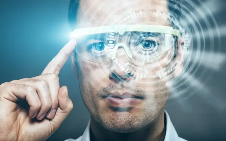
3D Imaging and Sensing
SCHOTT AF 32® eco is ideal as a substrate in infrared narrow band filters for 3D Imaging and Sensing. It’s also a vital component of Structured Light and Time of Flight (ToF) sensors, Stereoscopic Imaging and LiDAR, facilitating functions such as facial recognition, distance detection and scanning. Camera autofocus and video assist functions, 3D modeling, and augmented and virtual reality, are other key areas of use.
Learn more
Camera imaging
AF 32® eco is highly effective as a wafer-level packaging solution, and it plays a significant role in the area of camera imaging. As the CTE of AF 32® eco corresponds to that of a silicon wafer, it’s an ideal choice for silicon wafer covers. The highly flexible options offered by SCHOTT in terms of size, shape and thickness, along with the high and homogenous transmittance properties of AF 32® eco, make it an adaptable and reliable choice.
Learn more


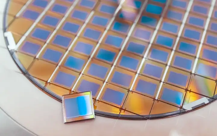
Semiconductors and MEMS
Given the compatibility of AF 32® eco with silicon components, it functions highly effectively in semiconductor systems. Silicon thinning is becoming an important process in semiconductor component manufacture, and AF 32® eco can be used as a temporary bonding solution with silicon. The same attributes enable it to act as a high-quality wafer-thin glass cover or substrate for MEMS applications.

RF and HF
AF 32® eco has a key role to play in applications involving RF (radio frequency) and HF (high frequency) devices, ranging from the smartphone market to wearable and automotive fields. With a low level of dielectric loss, AF 32® eco can be used as a substrate in SAW filters, converting electrical signals to acoustic waves and back again. These look set to play a key role in the growing 5G communications industry.
Microdisplays
Microdisplays such as LCoS, microOLED, and microLED rely on top-quality glass components such as AF 32® eco to achieve optimum performance. The ability of AF 32® eco to maximize optical transmission quality also makes it ideal for projectors, Near-To-Eye (NTE) devices, head-up and head-mounted displays, and electronic viewfinders, as well as augmented and virtual reality systems.