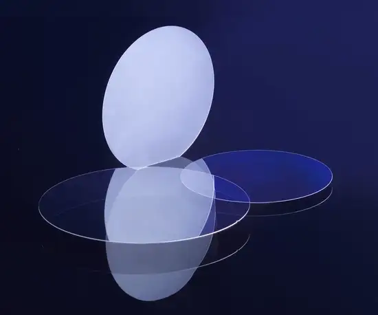
Product Variants of Substrates and Wafers
Unpolished substrates and wafers

CHARACTERISTICS
Due to very a low surface roughness below 0.5 nm and tight tolerances across our product range, the down-draw technique produces pristine surfaces perfectly suited for etching, coating and bonding.
YOUR ADVANTAGES
- Accurate and high-yield etching in semiconductor applications.
- Excellent transmission properties.
- Adhesion behavior makes it easy to apply substrate coatings.
- Wide range of glass types and thicknesses available, from 30 µm to 1.1 mm.
Polished substrates and wafers

CHARACTERISTICS
SCHOTT’s polished substrates and wafers offer an extremely low TTV below 0.6 µm, along with high flatness that ensures less warping or bowing of the glass. They are perfectly suited to wafer-level packaging and glass carrier wafer applications for 3D IC, RF IC, and wafer-level fan-out packaging. With a wide range of high-quality materials available from SCHOTT’s acclaimed portfolio, the possibilities are almost endless.
YOUR ADVANTAGES
- Extremely low TTV and superior flatness.
- Perfectly suited to highly precise 3D IC stacking processes.
- Various glass types available, enabling different bonding processes, such as temporary laser bonding, anodic bonding, and others.
- Also ideal as a substrate for wafer-level fan-out packaging.
- Outstanding dielectric properties.
