
Nanoimprint lithography. The art of precision at scale.
The revolution in optical manufacturing
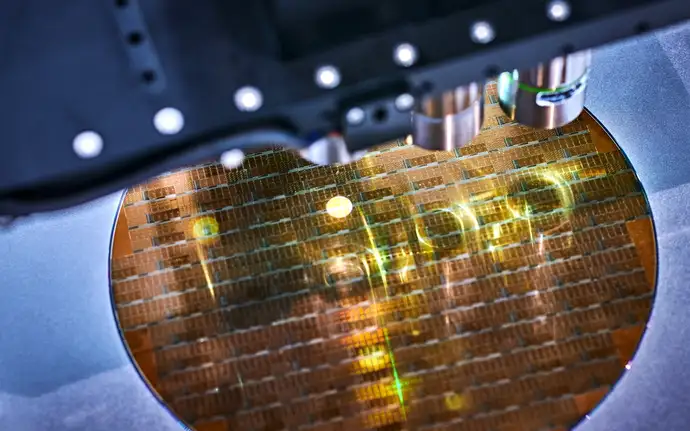
Nanoimprint lithography does not just replicate optical function, it redefines precision manufacturing. Diffractive optics, diffusers, microlens arrays, and metasurface-adjacent elements are no longer assembled, aligned, or fine-tuned. Instead, they are replicated at wafer scale with nanometer fidelity.This breakthrough enables thinner optical stacks, fewer components, and scalable high-volume production. Yet, it eliminates every classical correction mechanism. Once optical function is replicated, it cannot be tuned, realigned or compensated. Nanoimprint shifts optical performance from mechanical adjustment to material-defined geometry.
Why nanoimprint demands material intelligence
Modern optical components face relentless demands:
- Ultrathin and ultra-compact form factors
- Mass manufacturing at wafer and scale
- Uncompromising stability under optical and geometric sensitivity
Classical optics absorb variation through alignment, spacing, and calibration. But as systems shrink and stacks flatten, these buffers disappear entirely.
Nanoimprint emerges as the solution where alignment no longer scales. It replaces assembly precision with replicated surface functionality – and transforms optical performance from mechanical adjustment to material-defined geometry.
The physics of replication: What changes?
In nanoimprint, optical behavior is encoded into nanometer-scale surface structures. Phase control, beam shaping, and light distribution are baked directly into geometry.
There is no post-alignment. No calibration margin. No downstream correction. What is replicated defines optical behavior.
At the nanometer scale, deviations are not just amplified. They are directly transcribed into optical performance.
Industrial scaling: Where nanoimprint meets reality
Nanoimprint is not a theoretical marvel – it is a production reality. But scaling introduces critical challenges:- Edge-to-edge variation causes focus and phase non-uniformity across the wafer.
- Wafer warp and TTV amplify optical deviation across the full aperture.
- Surface defects are replicated millions of times, never to be rejected once.
- Thermal stress introduces irreversible drift during imprint, coating, or reflow
- Lot-to-lot variation compromises reproducibility and yield.

The indispensable role of glass in nanoimprint
In nanoimprint lithography, the substrate is not just a carrier. It is the architect of performance limits. Glass delivers a rare combination of properties that polymers and metals simply cannot sustain at wafer scale:

 ensure wafer-wide optical uniformity")

 support imaging and 3D
sensing performance")

SCHOTT: Enabling nanoimprint beyond prototypes
Anyone can imprint structures. Few can ensure they remain optically identical after millions of repetitions.SCHOTT materials are engineered for industrial-strength nanoimprint:
- Broad thickness ranges for diverse optical architectures
- Tight geometric tolerances and low warp for uniform replication fidelity
- High optical quality for imaging and 3D sensing
- Thermal and chemical robustness for stable process windows
- Consistent properties across melts and production lots

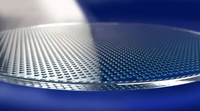
Glass substrates for nanoimprint: Where geometry defines function
Glass substrates power nanoimprint where optical function is fully defined by surface structure:
- Diffractive optical elements (DOE)
- Optical diffusers
- Microlens array substrates
- Structured substrates for projection and structured-light systems
- Substrates for metasurface-adjacent architectures
In each case, optical performance is determined before the first photon enters the stack.
SCHOTT glass materials that set the standard
Only a select few specialty glasses combine the optical, geometric, and thermal properties required for high-fidelity nanoimprint:D 263® T
Thin glass optimized for wafer-level nanoimprint and lithographic processes.With tight thickness tolerances, low TTV, and ultra-smooth surfaces, it enables high-fidelity replication of nanostructures. Exceptional transmission in visible and near-infrared ranges supports phase- and intensity-critical designs.
AF 32®
Thermally stable thin glass with a low coefficient of thermal expansion.Its homogeneous optical properties and thermal robustness preserve nanoscale structures during processing, reflow, and long-term operation, especially in temperature-sensitive applications.

BOROFLOAT® 33
Borosilicate glass offering unmatched thermal stability and smooth surface quality.Its extremely low surface roughness and thickness range, making it well suited for nanoimprint lithography applications. The high temperature resistance and low thermal expansion of BOROFLOAT® enable precise pattern transfer even under demanding proces.

When nanoimprint on glass is the only viable choice
Nanoimprint on glass is the gold standard where optical function, compact form factor, and volume scalability must coexist – without relying on correction mechanisms:
Automotive sensing

Industrial and smart systems
Where nanoimprint meets the future
Nanoimprint does not exist in a vacuum. It intersects with other domains where optical function is defined at wafer scale and material stability is performance-critical.
Wafer-level optics
Scaling optical function without alignment at wafer level.

Metalenses
When miniaturization leaves no room for error.
Discuss your nanoimprint requirements
Nanoimprint processes demand precise and stable material behavior to ensure consistent optical performance. Tell us about your application, and we will support you in selecting the right glass for reliable replication at scale.
