
Metalenses. When optical miniaturization leaves no room for correction.
Why metalenses?
Optical systems face relentless pressure to shrink in size, flatten in form, and integrate more seamlessly, all while meeting rising demands for higher resolution, tighter tolerances, and greater sensitivity.
Traditional refractive optics struggle under these constraints. Stack height increases, alignment becomes fragile and thermal drift grows more problematic, forcing designers to compromise between form factor and stability.
Metalenses step in where these trade-offs are no longer acceptable. They replace bulky, curved optics with ultra-thin, nanostructured surfaces. Instead of relying on lens shape and assembly, optical function is now defined by geometry etched directly into the material. The real question is not what metalenses are, but what happens when optical function is fixed permanently in structure.
Optical function fixed at material level
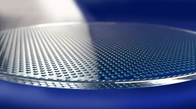
Metalenses manipulate light using sub-wavelength nanostructures that locally adjust phase and amplitude. Focusing, beam shaping and wavefront control are no longer shaped by curvature, but by the material’s own geometry. This enables ultra-flat components and simpler module layouts – but it also eliminates traditional correction mechanisms.Once fabricated, metalenses offer no room for adjustment. Phase errors cannot be compensated, misalignments cannot be corrected, and optical behavior cannot be recalibrated. Performance shifts from assembly precision to fabrication accuracy, making material-defined limits immediately visible at the optical level.

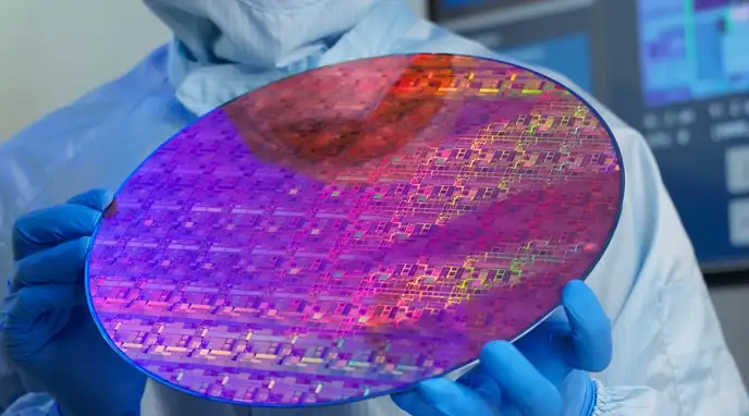
From simulation to production: The scaling challenge
Metalenses rarely fail in theory. They fail in practice – when scaled up. Nanometer-scale deviations that seem insignificant in simulations become critical in reality. Tiny geometric errors distort phase control. Thermal effects introduce wavelength-dependent shifts. Mechanical stress causes focus drift. Over time, performance degrades.The core challenge isn’t achieving peak performance; it’s ensuring stable, reproducible phase behavior across wafers, batches and the product’s entire lifespan. Many metalens concepts stall here – not at the prototype stage, but at reproducibility, yield, and long-term reliability.
The substrate: Where performance begins
In metalenses, optical function is defined at the sub-wavelength scale. At this level, material properties do not just influence performance – they define it. Once nanostructures are etched, material characteristics become optical parameters:


Manufacturing and integration: A shift in complexity
Metalenses become practical through scalable processes such as nanoimprint lithography or advanced wafer-level patterning. Here, material choice dictates the process window:
- Surface quality determines replication fidelity.
- Dimensional stability controls overlay accuracy.
- Defect density impacts yield.
- Substrate homogeneity ensures wafer-level consistency.
Flat optics do not eliminate system complexity – they relocate it. Metalenses must remain stable during integration and under defined environmental stress. Success depends on material compatibility across the entire optical stack.
Related enablement domains:
Wafer-level optics
Enables the integration of optical functions at wafer scale, ensuring alignment-free and reproducible system architectures. Material precision and uniformity define whether optical performance can be scaled reliably across wafers and production batches.
Nanoimprint lithography
Replicates nanostructured optical functions with high fidelity, enabling scalable manufacturing of metalens geometries. Material properties determine whether nanoscale structures can be reproduced consistently without loss of optical performance.
Where metalenses excel: Constraint-driven applications
Metalenses are not universal replacements for classical optics. They shine where system constraints rule out volumetric optics, alignment flexibility or downstream correction. In these cases, planar, structure-defined optics can simplify architectures – if material stability and manufacturing realities are addressed.
Key applications:

3D sensing (Structured light, ToF)

Infrared imaging in compact modules

Wearables and mobile devices

Automotive in-cabin sensing
Design trade-offs: The cost of structure-defined optics
Metalenses introduce real constraints that must be addressed early in design:
- Limited wavelength bandwidth
- Chromatic aberration challenges
- Efficiency losses (design-dependent)
- Higher costs at low volumes
These are not flaws. They are the trade-offs for embedding optical function in material structure rather than assembly.
Glass substrates for reliable metalens performance
Only select group of specialty glasses combine the optical, geometric, and thermal properties needed for reproducible metalens performance:D 263® T
Thin glass optimized for wafer-level nanoimprint and lithographic processes. Its tight thickness tolerances, low total thickness variation (TTV), and ultra-smooth surfaces enable high-fidelity replication of nanostructures. Stable refractive index behavior and high transmission in the visible and near-infrared ranges make it ideal for phase-critical metalens designs.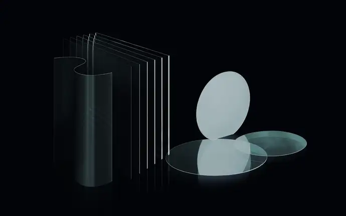
AF 32®
A thermally stable thin glass with a low coefficient of thermal expansion, comparable to silicon. As an alkali-free glass, it is fully compatible with semiconductor processes. Its homogeneous optical properties and thermal robustness help preserve nanoscale structures during processing, reflow, and long-term operation, particularly in temperature-sensitive integration scenarios.
BOROFLOAT® 33
Offers outstanding optical transmission from UV through VIS to NIR—particularly in the NIR range—making it an excellent substrate for metalens architectures. Its low autofluorescence supports applications requiring high signal-to-noise ratios and minimal background interference. The glass combines robustness against handling, chemical resistance, and thermal stability up to 450 °C, while being well proven in MEMS fabrication processes such as lithography. A wide range of thicknesses and substrate formats further enables precise and scalable metalens manufacturing.
Bridging the gap: From concept to industrial reality
SCHOTT does not design metalenses – we enable their industrial realization.
The SCHOTT Specialty Flat Glass Portfolio provides:
- Optically defined, reproducible substrates
- Wafer-level dimensional stability
- Ultra-smooth surfaces for nanoscale patterning
High transmission and controlled thermal behavior This ensures metalenses transition smoothly from design to stable, scalable production. For those industrializing metalenses, the focus must be on what truly drives performance: the long-term stability of the material beneath the structure.
Start your metalens project with us
Discuss material requirements, wafer-level integration, and scalable metalens production with SCHOTT experts.
