Technical Details of AF 32® eco
The alkali-free AF 32® eco is both environmentally friendly and technically impressive, with high transmission levels and excellent dielectric properties. With tight geometric tolerances and a CTE similar to that of a silicon wafer, this unique glass has a wide array of advantages for a large number of industries.
The eco-friendly answer to high technical demands
Material properties
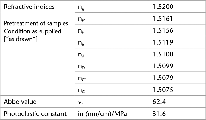
Optical properties
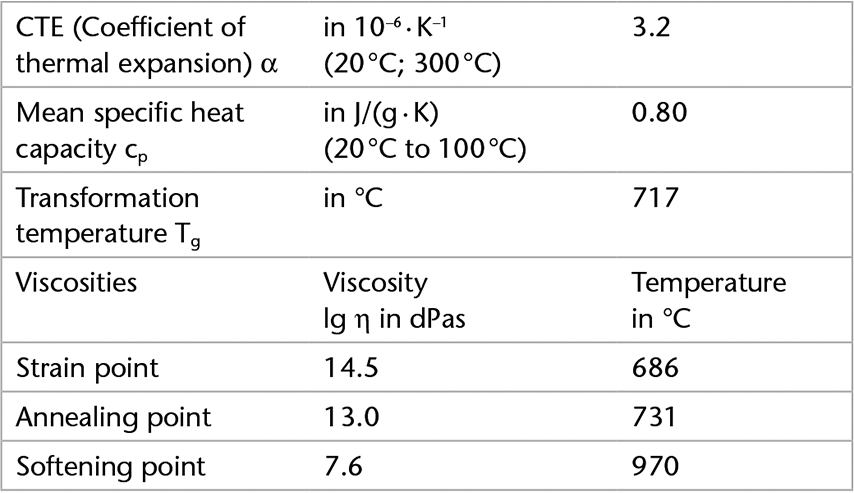
Thermal properties
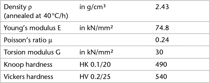
Mechanical properties
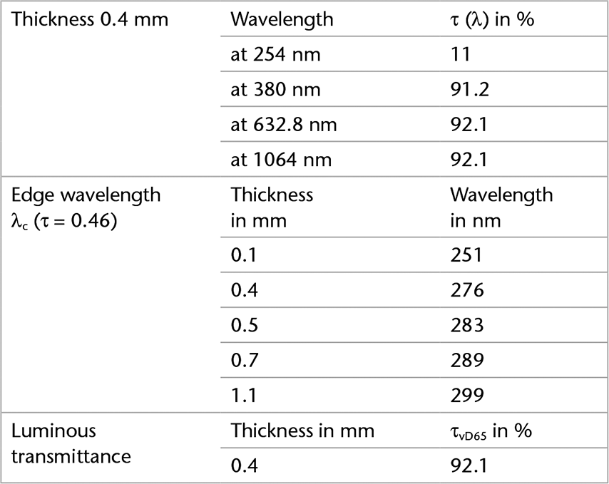
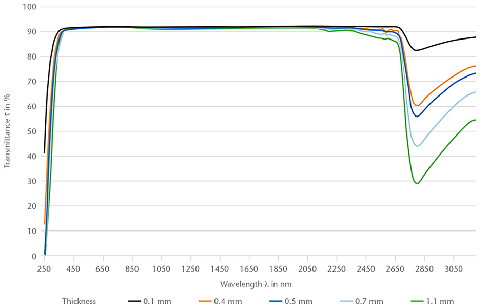
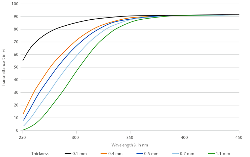
Transmittance values
Spectral transmittance (250 - 3150 nm)
Spectral transmittance (250 - 450 nm)
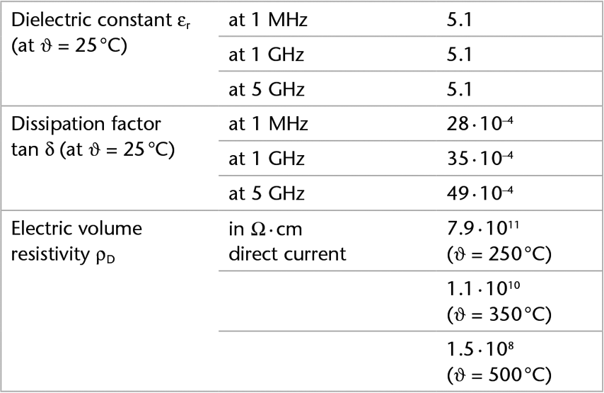
Electrical properties
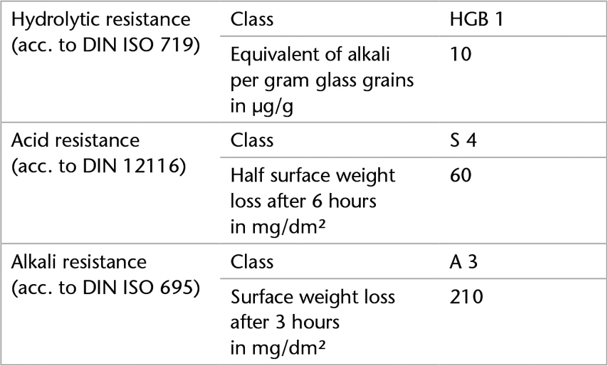
Chemical properties
AF 32® eco products
SCHOTT AF 32® eco is available as:
- Sheets
- Cut-to-size substrates
- Unpolished substrates and wafers
- FLEXINITY®
To find out more, please see the related products on the overview page.