Glass Carrier
What are glass carrier wafers?
Glass carrier wafers are precisely manufactured discs made of thin glass materials such as borosilicate and alumino-borosilicate. These materials are selected for their excellent thermal expansion properties and transmittance. Manufactured using advanced technology, the wafers meet stringent quality standards and are tailored to suit the specific requirements of the industry.
Why glass is ideal for semiconductors
In semiconductor manufacturing, carrier wafers and panels play a critical role. The advantages of glass over other materials include excellent thermal stability, which allows them to withstand high temperatures during processing without deformation. The stability of a glass carrier minimizes mechanical stress and maintains the integrity of the wafer during critical manufacturing steps. The diverse thermal expansion rates of available glasses also allow for optimal adaptation to various semiconductor materials, simplifying processing. Additionally, the high light transmission of glass aids precise optical inspections, essential for quality control. Together, these properties make glass an indispensable material for efficient and reliable semiconductor production.
Advantages of glass carrier
Glass carriers are becoming increasingly important in the fast moving world of semiconductors. This is due to the following key properties:
High raw glass quality
High reproducibility of our melting processes ensures high and consistent quality of raw glass.

Broad CTE range
This allows a range of materials to be placed as carrier wafers during semiconductor processing, with a closely matched CTE for optimal results.
Mechanical robustness
Excellent processing performance of carrier wafers results in extraordinary robustness in areas such as breakage strength.

Chemical and high temperature resistance
Glass is an excellent material for carriers thanks to its high resistance to acids and other chemicals, as well as its excellent thermal shock properties.

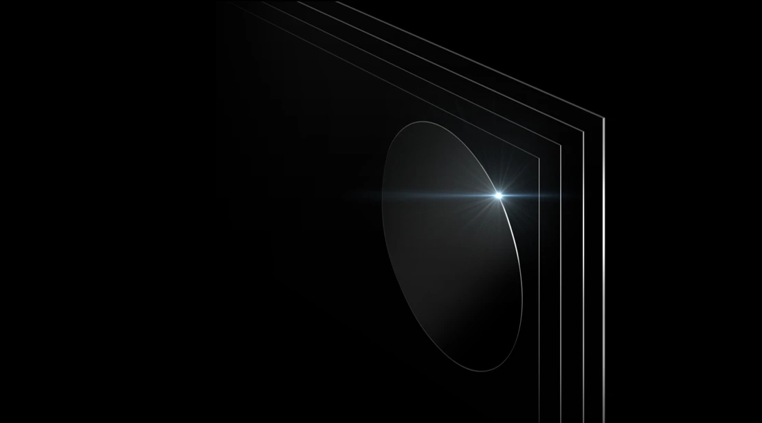
Transparency
The transparency of glass carriers enables a laser debonding process and allows in-process inspection. It also facilitates the identification of any bonding problems that may occur.

Extremely low tolerances
Carrier wafers offer a TTV level of ≤ 3µm, enabling superior silicon wafer thinning and a warpage of ≤ 50µm, avoiding higher warpage during the layer stacking process.

Form and shape
Glass is ideal as a carrier substrate as it offers fewer size limitations. Produced as a wafer, it has the same notch and chamfer geometry options as silicon wafers, with the added benefits of glass.

Cost-effective and durable
Thanks to its superior properties, glass carrier wafers and panels can be used up to 10 times, increasing the sustainability of these critical components while decreasing costs.

Ready for back-end processes
Glass carriers enable silicon wafer/die handling in semiconductor production.


Geometrical properties of SCHOTT Glass Carrier
| Geometrical properties | Value |
|---|---|
|
Ultra Low Total Thickness Variation (TTV) |
< 2.0 µm (Standard) |
|
Precise Thickness Tolerances |
± 5.0 μm (Standard) |
|
Warp (Depending on materials and thicknesses) |
8'' < 30 µm |
|
Cosmetic Quality (Depending on materials and thickness) |
Scratch/Digs: |
Bonding and debonding of glass carrier
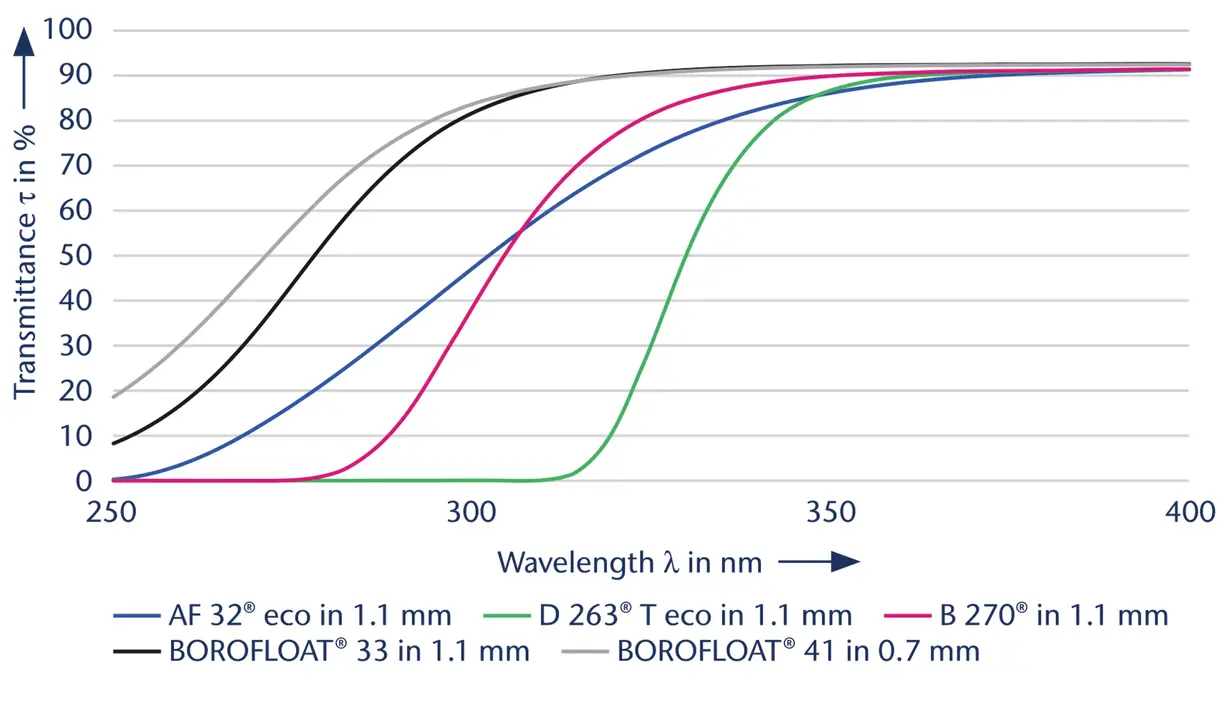
Spectral transmittance: thickness 1.1 mm for λ = 250 nm to 400 nm
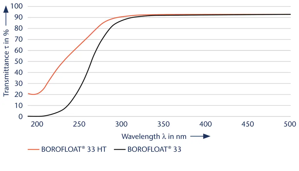
Spectral transmittance: thickness 1.1 mm for λ = 200 nm 500 nm
SCHOTT Glass Carrier can be delivered as follows:
- Flat/notch: According to SEMI standard
- Laser marking: According to SEMI standard, T7, QR-Barcode/unique number
- Cleaning: Ultra/mega-sonic cleaning and cleanroom ISO 6
- Packaging: Inspection and packaging under ISO 6 in wafer boxes (FOSB, RTU, etc.)