
Wafer-level optics: Precision at scale
When optical scaling meets material realities
Wafer-level optics represent a paradigm shift in optical system design, enabling the production of highly compact, scalable, and reproducible optical components. By fabricating hundreds or thousands of optical elements on a single wafer, this technology achieves unprecedented miniaturization. . However, it comes with a critical trade-off: the loss of corrective flexibility inherent in traditional optics.
In wafer-level optics, optical performance is locked in before calibration, software adjustments, or even the first pixel capture. Once the wafer is processed, any deviations are replicated across every element, leading to uniform signal degradation. This makes wafer-level optics fundamentally a material challenge, where the substrate dictates success.
The challenge: Scaling without a safety net
Unlike traditional optical assemblies – where alignment, spacing, and adjustments can compensate for imperfections – wafer-level optics do not offer such luxuries. Here, thousands of optical elements share a single foundation: the substrate.
Three critical factors influence optical signal integrity in wafer-level optics:
- Wafer-wide TTV and warpage: They create focus variations across sensor arrays, compromising uniformity.
- Cumulative misalignment: Stacked elements reduce signal fidelity before detection even begins.
- Thermal behavior: Temperature cycling shifts optical paths, destabilizing performance over time.
These factors collectively define yield, consistency, and long-term reliability.

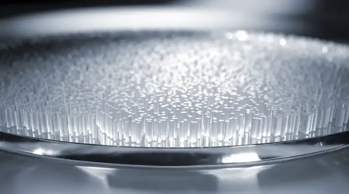
Glass: The backbone of wafer-level optics
In wafer-Level optics, whether for diffractive optic elements (DOE), diffusers, or microlens arrays, glass is not just chosen for its optical clarity. It is the key to stability, reproducibility, and scalability.
To succeed, the substrate must deliver:


Glass solutions for wafer-level optical components
Different applications require different substrate properties. The following high-performance glass materials are tailored for wafer-level optics:
D 263® T
With tight thickness tolerances, minimal total thickness variation, and superior surface quality, D 263® T supports high-fidelity replication, lithography, and optical stacking. Its stable refractive index and excellent transmission make it perfect for large-scale production.
AF 32®
The low coefficient of thermal expansion and homogeneous optical properties of AF 32® ensure alignment and performance stability through thermal cycling, reflow, and long-term operation – ideal for silicon-bonded applications.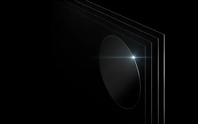
BOROFLOAT® 33
For architectures requiring excellent thermal compatibility with silicon. Its coefficient of thermal expansion (CTE) closely matches that of silicon, making BOROFLOAT® 33 particularly well suited for wafer-level optical systems where reliable bonding and dimensional stability are critical. This CTE match enables processes such as anodic bonding, providing a strong and hermetic alternative when adhesive or frit bonding are not suitable. In addition, BOROFLOAT® 33 supports a wide range of bonding approaches, from UV bonding to anodic bonding technologies.
Where wafer-level optics are in action
Wafer-level optics do not sense directly. They enable the compact, reproducible optical components that power modern sensing applications:

Imaging and sensing

Automotive sensing

Mobile sensing
The future: Structure over assembly
As wafer-level architectures advance, optical function is increasingly embedded in surfaces and geometries, replacing traditional assembly methods:
Metalenses
Optical function is embedded directly into nanostructures, eliminating the need for multi-element assemblies. Performance depends on how precisely geometry and material properties are controlled, with no possibility for post-production correction.

Nanoimprint lithography
Nanoimprint enables scalable replication of nanostructured optical functions across entire wafers. Material fidelity defines whether optical performance can be reproduced consistently without alignment or adjustment.
Start your wafer-level optics project
Discuss substrate requirements, manufacturing constraints and scalable optical architectures with SCHOTT experts.
