
Electronic packaging materials & design
What materials are used in electronic packaging?
Explore the broad variety of materials and their typical use cases:Adhesives and sealants:
In electronic packaging, adhesives and sealants like epoxy resin and silicone rubber are commonly used.
Epoxy offers strong bonding while silicone provides flexibility and resistance to moisture.
Composites:
Fiberglass epoxy (FR-4) is often used for printed circuit boards (PCBs) because of its electrical insulation properties.
Metal matrix composites combine metals with ceramics to create a material that is useful for heat sinks because of its improved thermal performance.
Metals:
Metals are a common material in electronic packaging. The specific metal used will depend on the conductivity, thermal properties, and environmental protection required.
Aluminum is often used for lightweight enclosures and heat sinks, while copper is good for electrical connections. Steel offers excellent structural support and shielding.
Nickel and tin are good choices for corrosion resistance, while gold is ideal for highly reliable connectors.
Various alloys like beryllium copper and magnetic alloys can also be useful for specialized applications.
Plastics:
Polyethylene, polypropylene, and polyvinyl chloride are often used for cost-effective electrical insulation and to protect electronic components from moisture and dust.
Polycarbonate — known for its impact resistance and transparency — is often used to make protective covers for devices with display screens.
Acrylonitrile butadiene styrene (ABS) offers a good balance of strength and impact resistance for enclosures and structural components.
Plastics such as polyetheretherketone (PEEK) are used to create moisture-blocking seals, yet are not hermetic.
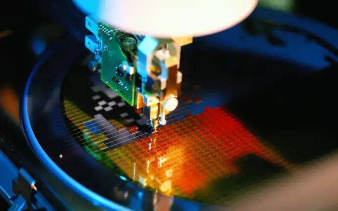
Synthetic resins such as acrylates or epoxies are widely used for transfer molding. The process involves heating the synthetic resin until it becomes pliable, and then forcing it into a mold cavity to encapsulate the semiconductor device.
Ceramics:
Alumina is used in packaging for electrical insulation and thermal conductivity.
Aluminum nitride has excellent electrical insulation and thermal management properties.
Another common ceramic is silicon carbide, which is known for its high thermal conductivity and use in high-power electronic devices.
Thermal interface materials:
These materials conduct heat when placed between solid surfaces. In a packaging context, thermal interface materials in the form of greases and pads are often applied between heat-generating components and heat sinks to prevent overheating by further improving heat transfer and temperature management.
Foams and gaskets:
Polyurethane and silicone foams are flexible and soft materials used for shock absorption and to provide a cushioned barrier. Gaskets — usually made of rubber, silicone, or neoprene — are used to prevent intrusion of moisture, dust, or electromagnetic interference.
Metallization and coatings:
Metallization or coating of electronic components can enhance functionalities such as electrical conductivity, corrosion resistance, and environmental protection. Gold, silver, and copper are often used to increase electrical conductivity while nickel, palladium, tin, and platinum can be used to improve oxidation, corrosion resistance, and aesthetic properties.
Glass:
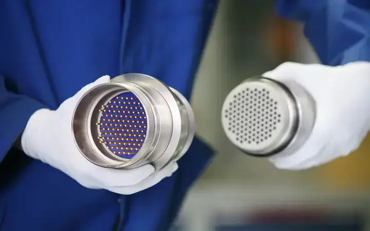
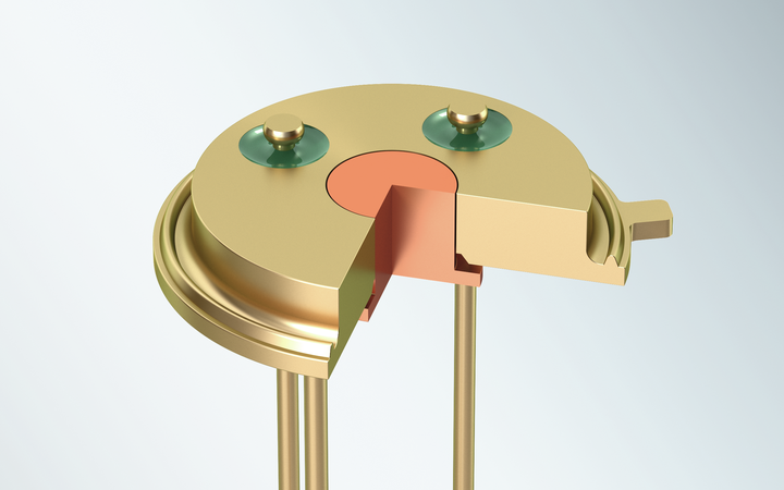
- Glass is a key component of hermetic glass-to-metal seals which combines different glass types with metals that have compatible coefficients of thermal expansion.
- For matched glass-to-metal seals — which are made using materials with similar thermal properties — Kovar, steel or stainless steel as well as alumina ceramic can be used.
- For compression glass-to-metal seals — where thermal differences are used to create a mechanically robust package — carbon steel, stainless steel, a nickel-chromium-based superalloy known as Inconel, and nickel iron are commonly used.
- Titanium or platinum are typically the materials of choice if biocompatibility is important. Glass and glass-to-metal sealing is not only used for the packaging, but also applied widely in optical windows, caps and covers.
Common glass types used in electronic packaging
- Offers high thermal resistance and a low coefficient of thermal expansion, making it suitable for applications where temperature changes are significant.
- Typical applications include hermetically sealed glass-to-metal components such as sensor packaging or connectors.
- Also known as quartz glass, fused silica offers favorable optical properties and high UV and infrared transparency.
- Typical applications include optical components, high-frequency devices, and semiconductor substrates.
Thanks to its thermal and mechanical properties, aluminosilicate glass is often used in use cases that require high robustness and shock resistance.
- Glass-ceramics combine the beneficial properties of glass and ceramics. Like glasses, they can be directly sealed with metals without any interface materials. They also offer thermal stability and mechanical strength comparable to ceramics.
- Applications include packaging components and sealing materials in high-temperature environments.
More about HEATAN® glass-ceramics.
- Often referred to as passivation layers or passivation coatings, passivation glasses are used in electronic packaging applications to add protective thin film layers to semiconductor devices and electronic components.
- These protective layers help prevent corrosion, increase reliability and resistance from environmental factors such as moisture, that could degrade the semiconductor’s performance.
- Passivation glasses are typically Pb-Si-Borate-, Zn-Borate or Borosilicate-glasses.
- More about SCHOTT Passivation Glasses
- Thanks to their low softening point (below 550°C), solder glasses (also known as frit glasses) enable the bonding of glass to ceramics, metals, or other glasses without causing thermal damage.
- The glass solder/bonding process involves applying the solder glass (usually in a powdered or preform state) to the surfaces to be joined and then heating them to the softening point. The glass liquefies, creating a bond upon cooling.
- Glass soldering is commonly used in applications such as opto-electronic packaging, MEMS packaging, and the sealing of display devices.
- More about SCHOTT Solder Glasses
- Some electronic packaging applications require special glass types with specific material properties, such as resistance to electrolytes, radiation, or glass types with a low dielectric constant (e.g., microelectronic applications).
SCHOTT offers hundreds of standard glass types, yet continues to develop new glasses for new applications and customer requirements.
- While sapphire is not a type of glass but a crystalline form of aluminum oxide, it offers similar properties to glass such as excellent optical transparency, hardness, and electrical insulation.
- In electronics packaging, sapphire is commonly used as a semiconductor substrate or to make optical windows and caps.
What is electronic packaging design?
When it comes to designing electronic packages, a multitude of factors come into play.In every design puzzle, the different pieces are most of all influenced by the environment in which the electronics will operate, including the temperature and pressure ranges.
Application-oriented design considerations include the voltage, current, and the frequency needed for the electrical feedthroughs. Preventing electrostatic discharge (ESD) as well as the compatibility with other materials are additional factors.
And in the background, the unsung heroes: manufacturability, size, and cost. Considering these elements will ensure that the design offers optimal performance, but also fits into the practical landscape.
Here is an overview of the most common critical design considerations:
Electrical
Electronic packages must exhibit signal integrity, power distribution, and electromagnetic compatibility. This requires designing for minimal signal loss, noise, and interference, while also creating efficient power distribution networks and managing electromagnetic interference. For some applications, the package must be designed to allow radio frequency signals to pass through or be equipped with optical windows that let specific wavelengths of light in and out. It can also be necessary to design the packaging in a way that blocks radio frequency noise emission and electrostatic discharge.
Mechanical
When it comes to mechanical factors it is critical to consider structural integrity, size, and material selection. Packaging must withstand physical stresses, fit within the space available, and use materials that enhance their strength and durability. The ability to easily assemble and service the device is also important for manufacturing and maintenance.
Thermal
Overheating can not only cause early failures but can also lead to safety issues. This makes it critical to manage temperature by designing heat sinks and thermal pathways and to select heat conductive materials.
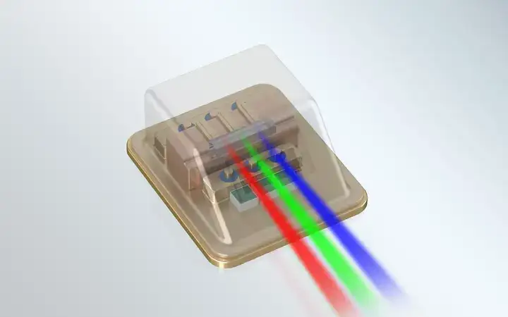
Optical
If a device uses optical components, then transparency, beam shaping, anti-reflective coatings, and light management are important considerations. For optimal performance, the package design must allow light or optical signals to pass through while minimizing glare and reflections.
What is SIP in electronic packaging design?
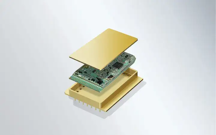
System-in-package (SIP) is an advanced packaging technology that integrates multiple integrated circuits (ICs) or electronic components — such as microcontrollers, memory chips, passive components, or sensors — into a single package. SIP is a subset of microelectronic packaging that allows more functionality in a smaller footprint, thereby enabling the development of high-performance electronic systems that are more compact and miniaturized. Variations include multi-chip module (MCM), package-on-package, and 3D packaging.
Although SIP methods can generally be used with various types of components, MCM packaging specifically integrates ICs. MCM packaging is often used when high performance, miniaturization, and enhanced system integration are essential. It is used for microprocessors, memory modules, and advanced electronic systems, such as smartphones, and high-speed data communication devices.
Advantages of MCM packaging in SIP technology


What is thermal management in electronic packaging?
Effective temperature management in electronic packaging design is essential to keep electronics within safe operating temperatures. Adequate heat dissipation can also improve the reliability and performance of devices and systems. For certain applications, the heat created by the electronics can damage the device or shorten its lifetime. For example, optical sensors and other imaging systems generate large amounts of heat because they acquire large volumes of data. For telecommunications lasers, better cooling enables higher-power lasers to be used without overheating.
A variety of packaging approaches can be used to keep electronics cool. For example, the device can be thermally bonded to the package to provide a thermal mass, thermoelectric coolers can be added between the component and the package, or materials such as aluminum nitride that have good conductivity can be used as insulators. Additionally, heat sinks can be brazed into electronic packages.
Key aspects of thermal management include:
- Design: Careful design of PCB layouts, selecting heat conductive materials, and optimized heat sinks can help achieve optimal airflow and prevent overheating.
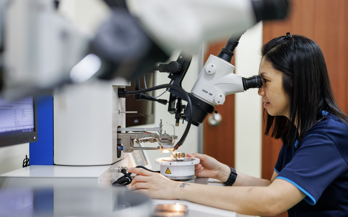
- Simulation and testing: Computer modeling and real-life, physical measurement and testing are essential to evaluate and validate the thermal performance of materials and components.
Common materials and components used to achieve thermal management
Heat sinks are metal components that absorb and dissipate heat, keeping it away from electronic components. They increase the surface area for heat transfer and are often combined with fans or other cooling methods.
Thermal interface materials include thermal pastes or thermal pads that can be placed between a component and a heat sink to improve thermal conductivity and reduce thermal resistance.
Active cooling systems such as thermo-electric coolers, fans, pipes, or liquid cooling can remove heat from electronic components.
Phase change materials change phase (e.g., from solid to liquid) at a specific temperature and can be used to absorb and release heat during the phase transition.
You may also like


Robert Hettler
Head of R&D Opto-electronics