Electronic packaging
Welcome to the world of electronic packaging. Whether you are new to the topic or an experienced engineer looking for detailed technical information, this webpage caters to all levels of expertise. It serves as a knowledge hub, providing a comprehensive resource for a range of audiences: from electronics engineers, manufacturers, or suppliers to tech enthusiasts.
If you want a recap of the basics, you can start at the beginning. For those who would like to dive deeper, you can directly move into technologies. Similarly, you can explore the subpages related to materials and design, as well as important aspects concerning reliability.
The future trends section offers you a sneak peek into exciting EP innovations that lie ahead. For information about the packaging solutions offered by SCHOTT, please visit the top products overview.
What is electronic packaging?
Electronic packaging is a term that can be applied to both the procedures involved in packaging electronics and the end products or systems that result from those processes.
It includes the design and manufacture of structures and enclosures that protect electronic components, semiconductor devices, and systems from physical damage, environmental stress, and electromagnetic interference while making sure they work properly. It also involves selecting the best materials and design to ensure durability of components and impart various functionalities such as preventing electrostatic discharge (ESD) .
Today, electronics packaging is an important part of everyday life, as the electric components, devices, and systems we rely on daily — from smartphones to computers, and more — all require some type of packaging.
When is electronic packaging useful?
Electronics packaging is a critical enabler for the performance, safety, and longevity of components and devices. Dive into its different use cases, from shielding against environmental threats to optimizing functionality, ensuring safety, and enhancing user experience:


What are some common applications where electronic packaging is important?
Today, electronics packaging is found almost everywhere — from wearable devices to satellites braving the harsh conditions in space. Because it plays a pivotal role in a vast and diverse number of fields, it is impossible to list all its uses on a single page.
Common applications include:


Electronic packaging technology
What are the various levels of electronic systems packaging?
Electronic systems packaging can be classified into hierarchical tiers. The level at which packaging takes place depends on factors such as the application needs, environmental conditions, size constraints, and cost considerations. Click on the plus signs in the below graphic to learn more about the different levels.
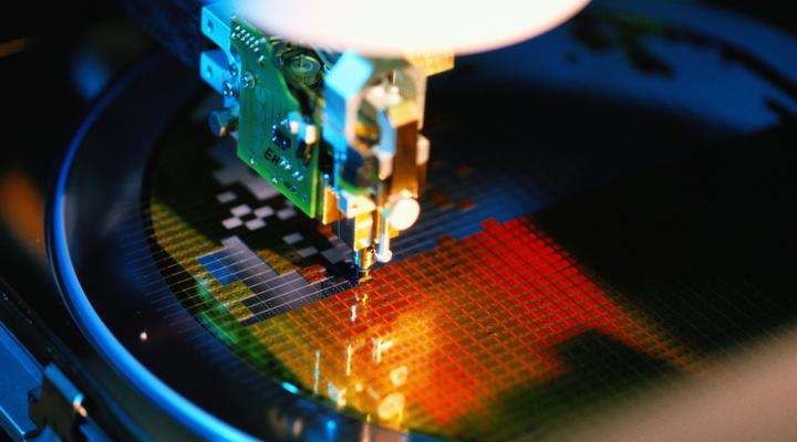
Wafer level
The semiconductor manufacturing process often begins with the processing of a silicon wafer, involving preparation, cleaning, and further steps to create integrated circuits. These steps may include photolithography and etching to define circuit patterns. After these processes, the wafer is diced into individual chips or dies, each of which is then ready for integrated circuit (IC) packaging.
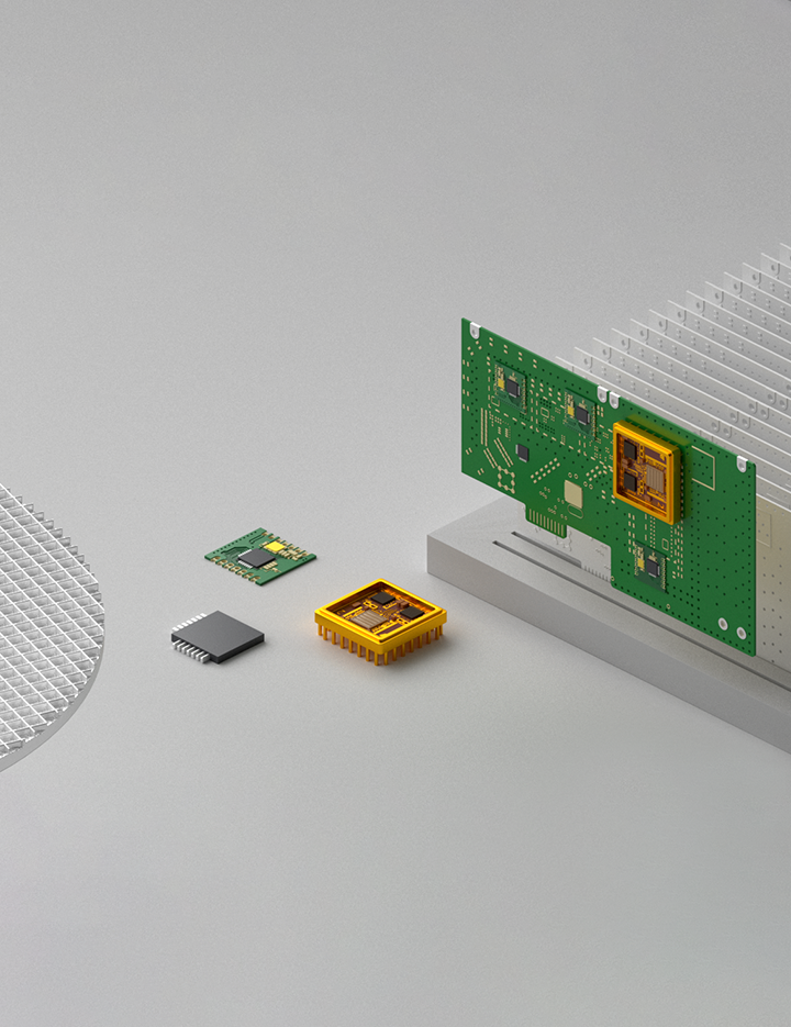
Level 0 – Integrated circuit (IC) chip
This level of packaging protects individual ICs, also known as microchips or dies. It can be non-hermetic or hermetic and provides electrical connections to the chip while also protecting it from mechanical and thermal stresses. Hermetic packaging provides the highest grade of protection against environmental factors while non-hermetic packaging offers a cost-effective option for less demanding use cases.
Level 1 – Component
For component-level packaging, individual components, such as ICs, transistors, diodes, and resistors, are enclosed in protective housings. This offers protection from physical damage, contamination, and electromagnetic interference. Hermetic packaging can be used for custom solutions that meet specific environmental, size, heat management, or operating requirements.
Level 3 – Module
At this tier, a functional module is fabricated by integrating multiple components, PCBs, or ICs onto a single substrate or motherboard. Module-level packaging streamlines assembly and testing and can boost performance and reliability for various types of modules, including memory modules, radio frequency modules, and power modules.
Level 4 - System
For system level packaging, an entire system or product is placed into a protective housing or enclosure. Multiple PCBs, modules, and subsystems can be integrated into a single housing to create systems that are essential for consumer electronics, industrial equipment, and other complex products.
Wafer level
Level 0 – Integrated circuit (IC) chip
Level 1 – Component
Level 2 – Printed circuit board (PCB)
Level 3 – Module
Level 4 - System
What are the different types of electronic packaging?
Types of packages can range from simple plastic housings to specialized ceramic or glass-to-metal packaging. The choice of packaging depends on many factors, including the component type and size, application requirements, heat dissipation considerations, electrical characteristics, and the manufacturing process. Another key question is whether a fully hermetic seal is needed.


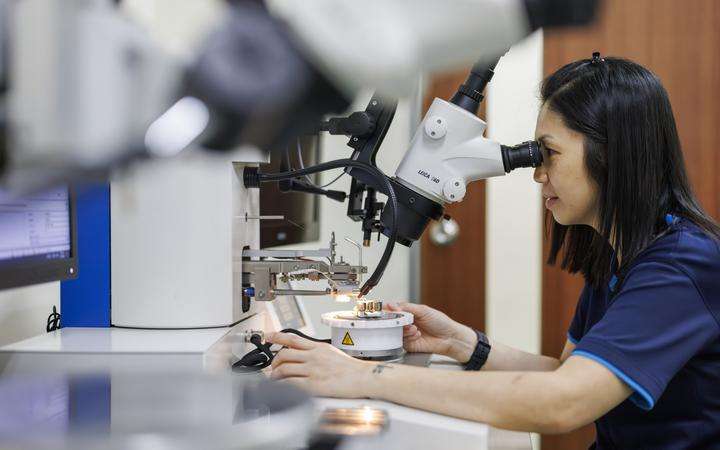
How are electronic packages made?
Electronic packages are made through a series of manufacturing processes designed to enclose and protect integrated circuits (ICs) and other components. At the same time, they need to provide electrical connections and ensure proper heat dissipation.
The manufacturing process varies for
-
Traditional IC packages:
Here, the chip is directly placed on the lead frame without the need for a cavity. Conductive epoxy materials, eutectic bonding, or soldering are used to mount the electronics on the respective carrier. A wire bonding or flip chip process is then used to connect the enclosed electronics to the conductors. The final step involves using encapsulation or overmolding to ensure no gas is left between the chip and encapsulation material. -
Cavity packages:
Certain housings, especially those used for optical components or micro-electro-mechanical systems (MEMS), may require a cavity to hold or mount the electronics and optics. Feedthroughs are integrated to allow electrical signals and power to pass through the enclosure. The environment inside the package can be room air, dry air, an insert gas, or a vacuum. Once the desired internal environment is obtained, the cavity is closed or sealed.
For traditional electronic packages, making the enclosure typically involves:

Future trends in electronic packaging
What is driving development in electronic packaging?
A number of factors influence the development of materials, designs, and manufacturing processes to meet the evolving demands of the electronics industry. Important drivers of innovation include miniaturization, reliability, and energy efficiency. Despite the continuous need to increase functionality and performance, there is also a simultaneous push to reduce costs.
When it comes to specific trends, one is to incorporate as much functionality as possible directly onto the semiconductor chip. System-on-chip (SoC) and system-in-package (SiP) approaches, for example, are being used to integrate a wide range of components and functions onto single chips for mobile or Internet of Things applications.
When multiple functions are integrated onto one chip, only one device — instead of many separate components — needs to be packaged. This simplifies the overall packaging process while also boosting performance, reducing power consumption, and shrinking the overall form factor.
There are also efforts to perform more packaging processes at the wafer level, where multiple chips can be processed simultaneously. This optimizes production efficiency and overall cost-effectiveness. It also further reduces the need for traditional packaging.
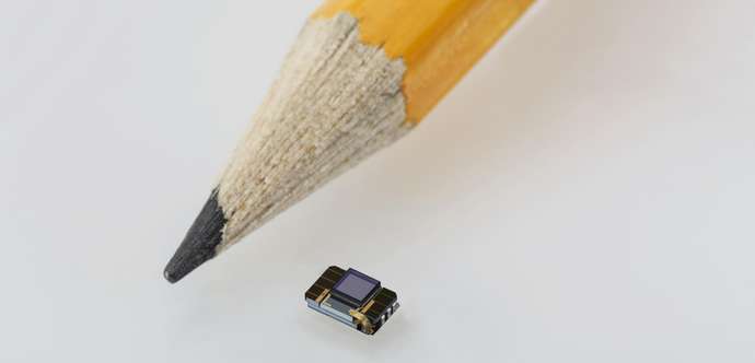
How can electronic packaging meet miniaturization requirements?
Miniaturization is one of the most important trends driving electronics packaging technology today. Whether it is a new medical device or the latest wearable technology, the boundaries are being pushed by the need for smaller, lighter, and more energy-efficient components.
As devices continually shrink, new approaches are being developed for creating packaging that is lightweight and compact while still delivering superior protection. These include chip stacking and 3D packaging, which optimize the use of limited space inside smartphones. As electronics get smaller, it has also become possible to seamlessly integrate them into fabrics and flexible substrates. This enables a range of completely new functions such as tracking vital signs and enhancing athletic performance. With these advancing technologies comes the need for new types of specialized, compact, and biocompatible packaging solutions to protect and integrate these electronics. The broader eco-conscious movement in consumer electronics has also brought a growing emphasis on using sustainable materials.
Conclusion
Electronic packaging is essential for not only protecting electronic components and devices but also ensuring their functionality and performance. By also encompassing heat management, electronical connections, interference reduction, and structural support, electronics packaging enables devices that are efficient, reliable, and suitable for a wide variety of industries. As electronics become ever more integrated into daily life, packaging solutions will continue to adapt to the need for improved performance, compactness, and sustainability.


Author: Robert Hettler, Head of R&D Opto-electronics
References
-
Roth, A. (1994), Vacuum sealing techniques, Oxford
-
Blackwell, G. (2017), The Electronic Packaging Handbook, IEEE Press
-
Harper, C., Miller, M. (1993), Electronic Packaging, Microelectronics and Interconnection Dictionary, McGraw-Hill, Inc.
-
John Lau, C.P. Wong, John L. Prince, Wataru Nakayama (1998), Electronic Packaging, Design, Materials, Process and Reliability, McGraw-Hill, Inc.
-
Schneider, S. (1991), Engineered Materials Handbook, Volume 4, Ceramics and Glasses, The Materials Information Society
Robert Hettler
Head of R&D Opto-electronics