
How Hisense is setting speed records with optical module technology
As one of the world’s leading optical communication device suppliers, Hisense Broadband Multimedia Technologies is putting the spotlight on its core optical communication technologies and ability to integrate industry segments. Its three-pronged capability in chips, modules, and terminals is helping the company gain new ground.
David Li is currently the Deputy General Manager and CTO of Hisense. Having obtained his Ph.D. from the University of Electronic Science and Technology of China, and the University of Houston, he joined Hisense in 2003 and began the development and industrialization of the company's optical communication technology. He has led the rapid development of Hisense for more than 10 years.
How has Hisense withstood the turbulence brought about by COVID?
Under the pandemic, the industry supply chain was greatly affected. However, there are opportunities in the crisis. With worldwide populations being home-bound, demand for internet traffic soared. From online shopping to online education, the building of broadband and data center infrastructure did not come to a halt. We had already resumed production in early 2020, and the company’s overall business was minimally affected. We were also leading the industry in product delivery capacity. Last year, Hisense grew by about 40 % in the field of optical communication.
What is your opinion on the current market environment?
In recent years, China’s domestic optical module industry has made significant progress, gradually surpassing foreign competitors. If you look at the statistics in recent years, about 80 % of the optical modules in the global market are produced in China. We are all making good progress, and the major players in the industry have made investments in optical devices and chips. Hisense, as one of the pioneer companies to invest in photonic chips, has developed vertically integrated manufacturing – one of our key competitive advantages.
What is the next growth area?
400G in Datacom, including 800G, 1.6T and 3.2T in the near future, are obvious growth areas. The wireless field has grown rapidly in China’s domestic market since 2019, and has transitioned from the original 25G gray light to color light. In Access Network, 10G EPON, XGPON, and XGSPON are replacing GPON and EPON from previous years. The recent domestic push for 10G PON for Internet Plus initiatives will also drive demand this year. According to market trends and our manufacturing expansion plan, we will be making significant investments. After 400G, Hisense invested a lot more into testing equipment, fine coupling equipment, and packaging equipment.
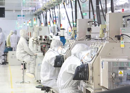
Hisense uses the latest equipment to produce a range of products for the optical communication industry
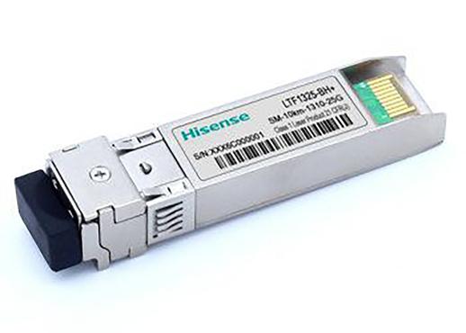
The 25G SFP28 LR transceiver is one of Hisense's key products
Why is packaging so important for optical modules?
The main function of an optical module is electro-optic conversion and photoelectric conversion. As speed and transmission distance increase, packaging technology will play an increasingly important role. With the speed increased, the power budget and requirements remain unchanged while bandwidth is increased, hence sensitivity gets worse. In 400G or 1.6T, 3.2T CPO optical modules, the coupling accuracy, consistency, and quality of the entire packaging will make up an increasingly crucial part of optical communication technology.
So packaging technology will become a key differentiator for optical modules in the future?
Yes. Building on core devices, packaging technology provides great competitiveness for optical modules. In the future, especially for high-speed optical modules, packaging will play an increasingly important role.
What do you think of the TO packaging format breaking its supposed speed limit again and again?
SCHOTT has been in a leading position in the field of TO packaging, driving technological progression in the entire industry. From 2.5G and 10G, up to 25G, SCHOTT has always been ahead. For the next generation of 50G and 100G applications, I am very much looking forward to even better products from SCHOTT, to provide excellent signal quality for high-speed applications, as they always have. In technological innovation, we have a positive and open attitude to collaborate with key strategic suppliers.
Text: Xingzhi Gu, FINN Partner
All photos: from Hisense website
Dec 12, 2021
Robert Hettler
Head of R&D Opto-electronics